PCB Impedance Control: PCB Design, PCB Manufacturing & High-Speed Signal Integrity
Modern electronic devices continue to become smaller, faster, lighter, and more functionally complex. Computers, smartphones, servers, storage systems, networking equipment, automotive electronics, industrial controllers, and other electronic products all depend on high-performance printed circuit boards (PCBs).
As signal edge rates become faster, simply connecting two components with a copper trace is no longer sufficient. A PCB trace can behave as a transmission line, and its geometry and surrounding dielectric structure can significantly affect signal integrity.
For this reason, PCB impedance control has become an important part of modern PCB Design and PCB Manufacturing.
Controlled impedance helps maintain predictable signal behavior between the source and load. When the characteristic impedance of a transmission line is properly matched to the intended system architecture, designers can reduce reflections, ringing, crosstalk, and other signal-integrity problems.
Although impedance control was historically associated primarily with high-speed digital and RF circuits, today’s high-density electronic systems increasingly require careful consideration of signal integrity even at relatively moderate clock frequencies because the signal edge rate, rather than clock frequency alone, determines whether transmission-line effects become significant.
What Is Controlled Impedance?
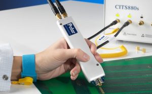
Controlled impedance refers to designing and manufacturing a PCB transmission line so that its characteristic impedance remains within a specified target and tolerance.
A PCB with transmission lines designed and manufactured to meet specified impedance requirements is commonly referred to as a controlled impedance PCB.
Characteristic impedance is determined by the electromagnetic relationship between the signal conductor and its return path. Important variables include:
- Trace width
- Trace thickness
- Dielectric thickness
- Dielectric constant
- Copper surface profile
- Reference-plane geometry
- Trace-to-plane spacing
- Differential-pair spacing
- Manufacturing tolerances
Controlled impedance is particularly important for:
- High-speed digital interfaces
- RF and microwave circuits
- Differential signaling
- DDR memory
- PCIe
- USB
- Ethernet
- SerDes
- High-speed networking
- High-frequency instrumentation
The objective is not simply to make every PCB trace have the same impedance. Instead, the target impedance should be defined according to the interface, component requirements, stackup, transmission-line topology, and system architecture.
Why Is Controlled Impedance Necessary?
A signal travels from a source through a transmission path to a receiving load. If the impedance changes abruptly along this path, part of the signal energy can be reflected toward the source.
The magnitude of the reflection depends on the impedance discontinuity.
For a simple load reflection, the reflection coefficient can be expressed as:
Γ = (ZL − Z0) / (ZL + Z0)
where:
- Γ = reflection coefficient
- ZL = load impedance
- Z0 = characteristic impedance of the transmission line
When ZL equals Z0, the idealized reflection coefficient is zero.
When the impedances differ significantly, more signal energy is reflected. These reflections can produce ringing, overshoot, undershoot, timing uncertainty, and other signal-integrity problems.
Therefore, impedance control is not simply a matter of selecting a trace width. It requires coordinated control of the PCB stackup, material properties, trace geometry, component interfaces, vias, connectors, and termination strategy.
When Does a PCB Trace Behave Like a Transmission Line?
One common mistake is to determine whether impedance control is necessary based only on the clock frequency.
The more relevant parameter is the signal’s rise time or fall time.
A practical rule is to compare the signal’s rise time with the propagation delay of the interconnect. If the propagation delay becomes a significant fraction of the signal transition time, transmission-line effects need to be considered.
A commonly used engineering guideline is to treat an interconnect as electrically long when its propagation delay is on the order of roughly one-sixth to one-third of the signal rise time, depending on the application and required accuracy.
This means a signal with a very fast edge can require transmission-line analysis even if its nominal clock frequency is relatively low.
For this reason, modern PCB Design should evaluate signal edge rate, interconnect length, dielectric properties, topology, and interface specifications rather than relying on frequency alone.
How Is PCB Impedance Controlled?
PCB impedance control generally involves two interconnected areas:
- Component and system-level impedance matching
- Transmission-line impedance control
Both must be considered together.
1. Impedance Matching Through Components
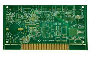
PCB traces cannot compensate for every impedance discontinuity created by components.
The source output impedance, receiver input impedance, connector impedance, package parasitics, and termination components all influence signal behavior.
Depending on the interface, designers may use:
- Series termination
- Parallel termination
- Thevenin termination
- AC termination
- Differential termination
- Source termination
For example, a series resistor near a driver can sometimes be used to increase the effective source impedance and reduce reflections on a single-ended transmission line.
The appropriate termination method depends on the interface and signal topology. It should therefore be determined during schematic and signal-integrity analysis rather than added arbitrarily during PCB layout.
2. Impedance Matching Through PCB Routing
The PCB transmission line itself must be designed to achieve the specified characteristic impedance.
The main parameters include:
- Trace width
- Copper thickness
- Dielectric thickness
- Dielectric constant
- Reference-plane distance
- Differential-pair spacing
- Copper roughness
- Trace geometry
For a controlled-impedance PCB, the designer typically specifies a target impedance and tolerance, such as a single-ended or differential impedance requirement.
The PCB manufacturer then uses the actual stackup and fabrication capabilities to determine the required trace geometry.
Types of Controlled PCB Impedance
Several transmission-line configurations are commonly used in PCB design.
Single-Ended Impedance
A single-ended trace is referenced to a nearby ground or power plane.
The impedance depends on the trace geometry and its relationship with the reference plane.
Differential Impedance
A differential pair consists of two traces carrying complementary signals.
The differential impedance depends on:
- Individual trace impedance
- Trace width
- Trace spacing
- Dielectric thickness
- Dielectric properties
- Copper thickness
Differential impedance is especially important for interfaces such as USB, PCIe, Ethernet, LVDS, and high-speed SerDes.
Single-Ended Coplanar Impedance
A coplanar transmission line has a reference conductor on the same PCB layer as the signal trace, in addition to a reference plane beneath it when applicable.
The distance between the signal trace and adjacent copper affects the resulting impedance.
Differential Coplanar Impedance
A differential coplanar structure combines differential-pair routing with coplanar reference copper.
This structure is commonly considered in RF, microwave, and high-speed PCB designs where controlled electromagnetic fields are important.
PCB Stackup and Controlled Impedance
One of the most important aspects of impedance-controlled PCB Design is the layer stackup.
A signal trace requires a predictable return-current path. In a typical multilayer PCB, this means routing the signal close to a continuous reference plane.
A simplified structure might look like:
Signal Layer → Dielectric → Ground Plane
The dielectric thickness between the signal and reference plane has a major effect on characteristic impedance.
If the dielectric spacing increases while other parameters remain constant, the trace impedance generally changes. The exact relationship depends on the transmission-line geometry.
Therefore, designers should establish the stackup before completing critical high-speed routing.
Why the Return Path Matters
High-frequency signal current does not simply travel through the signal trace and randomly return through the PCB.
The return current tends to follow the path of lowest impedance, which for many PCB structures is concentrated near the corresponding reference plane.
If a high-speed trace crosses a split, gap, or discontinuity in its reference plane, the return current may be forced to take a longer path.
This can increase:
- Loop area
- Electromagnetic radiation
- Crosstalk
- Impedance discontinuity
- EMI risk
- Signal-integrity problems
Therefore, maintaining a continuous reference plane beneath critical high-speed traces is one of the fundamental principles of controlled-impedance design.
Important PCB Stackup Parameters
A controlled-impedance stackup includes more than simply arranging signal and ground layers.
Important parameters include:
Copper Thickness
Copper thickness influences trace resistance, current-carrying capability, etching behavior, and the final transmission-line geometry.
Dielectric Thickness
The distance between the signal trace and reference plane strongly affects impedance.
Dielectric Constant
The dielectric constant, commonly represented as Dk, affects electromagnetic propagation through the PCB material.
The effective dielectric constant seen by a transmission line is influenced by the transmission-line geometry and the materials surrounding the conductor.
Copper Roughness
Copper surface roughness can increase conductor loss at high frequencies because of skin-effect-related behavior.
This becomes increasingly important in high-speed and RF applications.
Trace Width
Trace width is one of the most important geometry parameters used to achieve the target impedance.
Differential-Pair Spacing
For differential routing, the spacing between the two conductors affects their mutual electromagnetic coupling and therefore their differential impedance.
PCB Impedance Calculation
PCB impedance can be estimated using analytical equations, empirical formulas, or electromagnetic field solvers.
For simple structures such as microstrip and stripline, approximate equations can provide useful initial values.
However, high-speed PCB designs often require more accurate calculations because real PCB structures include:
- Copper thickness
- Copper roughness
- Resin distribution
- Frequency-dependent dielectric properties
- Etching geometry
- Trace sidewall profile
- Differential coupling
- Manufacturing tolerances
IPC-2141
IPC-2141 provides commonly referenced approaches for estimating impedance of certain PCB transmission-line structures.
However, simplified equations may not fully capture the behavior of advanced high-speed or high-frequency structures.
Therefore, IPC-based equations should be treated as engineering approximations rather than universal substitutes for electromagnetic field solving.
Field Solvers
For demanding high-speed and RF applications, a 2D or 3D electromagnetic field solver can provide a more accurate estimate.
Field solvers can account for:
- Actual trace geometry
- Dielectric thickness
- Material Dk
- Copper thickness
- Copper roughness
- Differential coupling
- Frequency effects
Manufacturers can then use these calculations to establish a practical impedance-controlled trace width and spacing for production.
Etching Factor and PCB Impedance
The PCB etching process influences the final trace geometry.
During copper etching, the sidewalls of a trace are not always perfectly vertical. The resulting trace may have a trapezoidal cross-section.
This means the width measured at the top of the conductor may differ from the width at the bottom.
An idealized etching factor can be represented using the relationship between copper thickness and the difference between the top and bottom trace widths.
One commonly used definition is:
Etching Factor = T / [(W1 − W2) / 2]
where:
- T = copper thickness
- W1 = wider trace dimension
- W2 = narrower trace dimension
The exact definition and measurement convention can vary by manufacturer, so engineers should confirm the manufacturer’s methodology before using an etching-factor value in impedance calculations.
This is important because the actual cross-sectional geometry of the trace affects the final characteristic impedance.
Impedance Control in Rigid-Flex PCB Design
Rigid-flex PCBs require additional attention because the transmission-line structure can change between rigid and flexible regions.
Factors affecting impedance include:
- Flexible dielectric material
- Rigid laminate
- Copper thickness
- Coverlay thickness
- Adhesive thickness
- Dielectric constant
- Trace width
- Reference-plane structure
- Overall flex thickness
A trace that has a controlled impedance in the rigid region may not have the same impedance in the flexible region if the surrounding dielectric structure changes.
Therefore, rigid-flex PCB Design should treat each electrical region separately and verify the transmission-line geometry across transitions.
Backdrilling and Via Stub Control
Vias can introduce impedance discontinuities into high-speed transmission lines.
A through-hole via may extend beyond the layer where the signal terminates, creating an unused section known as a via stub.
At high data rates, a long via stub can behave as a resonant structure and contribute to signal-integrity problems.
Backdrilling can remove part of the unused via barrel, reducing the stub length.
Other technologies, such as blind vias and microvias, can also reduce unnecessary via structures depending on the PCB architecture.
Therefore, via design should be included in the overall impedance-control strategy rather than considered separately from routing.
Complex Impedance and AC Circuit Behavior
PCB impedance should not be confused with the characteristic impedance of a transmission line.
In AC circuit analysis, impedance is a complex quantity:
Z = R + jX
where:
- R = resistance
- X = reactance
- j = imaginary unit
For an ideal inductor:
ZL = jωL
For an ideal capacitor:
ZC = 1 / (jωC)
where:
- ω = 2πf
- L = inductance
- C = capacitance
The real part represents resistance, while the imaginary part represents reactance.
This complex impedance is useful for analyzing components, filters, termination networks, and AC circuits.
However, it should not be directly equated with the characteristic impedance of a PCB transmission line. Characteristic impedance is a distributed transmission-line property, whereas component impedance is generally discussed as a frequency-dependent lumped or network parameter.
Keeping these concepts separate helps avoid confusion during high-speed PCB Design.
Why Is Impedance Control Important in HDI PCBs?
HDI PCBs often contain fine lines, microvias, closely spaced layers, and high-density components.
As routing density increases, maintaining predictable electromagnetic behavior becomes more challenging.
Controlled impedance is particularly important in HDI applications because:
- High-speed signals may pass through multiple buildup layers.
- Microvias can introduce local discontinuities.
- Fine traces are sensitive to manufacturing variations.
- Small dielectric-thickness changes can affect impedance.
- Dense routing increases crosstalk risk.
- BGA escape routing often requires tightly controlled geometry.
For these reasons, impedance control should be integrated into the complete HDI stackup and fabrication strategy.
Benefits of PCB Impedance Control
Proper impedance control can provide several important benefits.
1. Improved Signal Integrity
Controlled transmission-line impedance helps reduce reflections and ringing, supporting cleaner signal waveforms.
2. Reduced Crosstalk
Appropriate trace spacing and reference-plane structures reduce unwanted electromagnetic coupling between adjacent signal lines.
3. More Predictable High-Speed Performance
A controlled transmission environment makes signal behavior more predictable across the PCB.
4. Reduced EMI Risk
Maintaining a continuous return path and minimizing impedance discontinuities can help reduce unwanted electromagnetic radiation.
5. Improved Timing Margin
Signal reflections and ringing can shift threshold crossings. Better signal integrity can therefore improve timing margins in high-speed interfaces.
6. Reliable Differential Signaling
Proper differential-pair geometry helps maintain the intended differential impedance and signal balance.
7. Better System Reliability
For demanding applications such as automotive, medical, aerospace, telecommunications, servers, and industrial electronics, controlled impedance contributes to predictable system-level electrical performance.
PCB Manufacturing Considerations for Controlled Impedance
A PCB design can specify a target impedance, but the final result depends on manufacturing accuracy.
A manufacturer must control:
- Laminate thickness
- Prepreg thickness
- Resin content
- Copper thickness
- Copper roughness
- Trace width
- Etching compensation
- Layer registration
- Differential-pair spacing
- Final board thickness
For this reason, impedance control requires close cooperation between the PCB designer and manufacturer.
A practical manufacturing workflow may include:
- Define the target impedance.
- Select the PCB material system.
- Establish the stackup.
- Calculate the initial trace geometry.
- Review the design with the PCB manufacturer.
- Apply manufacturing compensation.
- Fabricate test coupons.
- Measure the finished impedance.
- Compare the results with the specified tolerance.
- Adjust the process if necessary.
Impedance Testing in PCB Manufacturing
For production PCBs, manufacturers can use dedicated test coupons to verify impedance.
Common measurement technologies include:
- Time Domain Reflectometry (TDR)
- Time Domain Transmission (TDT)
- Other appropriate high-frequency measurement methods
TDR is particularly useful because it can identify impedance variations along a transmission line and reveal discontinuities.
The test coupon should represent the relevant production stackup and trace geometry as closely as possible.
This provides a more meaningful verification of the actual manufactured PCB than relying solely on theoretical calculations.
Common PCB Impedance-Control Mistakes
Routing Before Finalizing the Stackup
Changing the stackup after routing can invalidate carefully calculated trace widths.
Ignoring the Return Path
A signal trace with the correct nominal impedance can still exhibit signal-integrity problems if its return path is interrupted.
Using Frequency Alone
Signal edge rate is often more relevant than clock frequency when determining whether transmission-line effects must be considered.
Ignoring Manufacturing Tolerances
Nominal trace width and dielectric thickness are not the same as the dimensions achieved on the finished PCB.
Crossing Plane Splits
High-speed signals should not cross reference-plane gaps without an appropriate return-current strategy.
Excessive Via Stubs
Long via stubs can become problematic as signal rise times become faster.
Assuming Every FR-4 Material Has the Same Dk
Different FR-4 material systems can have different dielectric properties, and the effective Dk depends on frequency and transmission-line geometry.
Treating Differential Pairs as Ordinary Traces
Differential impedance depends on both individual trace geometry and coupling between the pair.
PCB Impedance Control Design Checklist
Before releasing a high-speed PCB for manufacturing, engineers should verify:
- Target impedance is clearly specified.
- PCB stackup is finalized.
- Dielectric thickness is controlled.
- Material Dk/Df requirements are defined where necessary.
- Trace width is compatible with the selected stackup.
- Differential-pair spacing is controlled.
- Reference planes are continuous.
- High-speed signals have appropriate return paths.
- Plane splits and gaps are avoided or properly managed.
- Via stubs are evaluated.
- Copper roughness is considered for very high-speed signals.
- Manufacturing tolerances are included.
- Impedance test coupons are defined when required.
- TDR or an appropriate impedance measurement method is available.
- The PCB manufacturer has reviewed the stackup and impedance requirements.
How Kingda Supports Controlled-Impedance PCB Manufacturing
Controlled-impedance PCB fabrication requires coordination between PCB Design and PCB Manufacturing.
The design team should provide clear requirements for target impedance, tolerance, stackup, material system, layer assignment, differential-pair requirements, and critical interfaces.
A PCB manufacturer such as Kingda can review the proposed stackup and manufacturing data to determine whether the specified impedance targets are compatible with the available fabrication process.
For demanding high-speed designs, the manufacturing process should also consider actual copper thickness, dielectric thickness, etching behavior, trace geometry, registration, and test-coupon requirements.
This engineering collaboration is particularly important for HDI, high-speed digital, RF, networking, automotive, medical, and other reliability-sensitive PCB applications.
Conclusion
PCB impedance control is a fundamental part of modern high-speed PCB Design and PCB Manufacturing. As electronic systems become faster and more densely integrated, signal integrity can no longer be treated simply as a schematic-level issue.
Controlled impedance depends on the complete transmission-line structure, including trace width, copper thickness, dielectric thickness, dielectric properties, reference-plane geometry, differential-pair spacing, copper roughness, vias, and manufacturing tolerances.
Effective impedance control also requires a predictable return-current path. A theoretically correct trace width cannot guarantee good signal integrity if the reference plane is interrupted or if the transmission path contains significant discontinuities.
For high-speed and HDI PCBs, engineers should establish the stackup early, define impedance targets clearly, evaluate signal edge rates, control transmission-line geometry, consider via structures, and work closely with the PCB manufacturer.
By combining accurate PCB Design, appropriate materials, controlled fabrication processes, and impedance verification, manufacturers can produce PCBs capable of supporting high-speed data transmission, reliable signal integrity, and demanding electronic applications.
Article Summary
This guide explains PCB impedance control, including controlled-impedance principles, transmission-line behavior, impedance matching, PCB stackup design, return-current paths, trace geometry, etching effects, field-solver calculations, complex impedance, HDI impedance control, and manufacturing verification. Proper impedance control is essential for maintaining signal integrity and reliable performance in modern high-speed PCB applications.