Standard PCB Copper Thickness: PCB Design, PCB Manufacturing & Copper Weight Guide
Copper thickness is one of the most important factors affecting the electrical, thermal, mechanical, and manufacturing performance of a printed circuit board (PCB). The copper layer provides the conductive paths that connect components, distribute power, carry signals, and transfer heat across the board.

Selecting the appropriate PCB Copper Thickness is therefore an important part of both PCB Design and PCB Manufacturing. A copper layer that is too thin may not provide sufficient current-carrying capacity, while unnecessarily thick copper can increase material costs, affect fine-line routing, and make etching and plating more challenging.
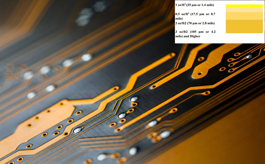
PCB copper thickness is commonly specified in ounces per square foot (oz/ft²), usually abbreviated as oz. Copper weight can also be expressed as micrometers (µm) or mils, where 1 mil equals 0.001 inch.
As a general conversion:
- 0.5 oz ≈ 17.5 µm ≈ 0.7 mil
- 1 oz ≈ 35 µm ≈ 1.4 mil
- 2 oz ≈ 70 µm ≈ 2.8 mil
- 3 oz ≈ 105 µm ≈ 4.2 mil
- 4 oz ≈ 140 µm ≈ 5.5 mil
These values represent nominal copper thickness before accounting for manufacturing processes such as electroplating. The final copper thickness can therefore differ depending on the PCB fabrication process and whether additional copper is plated onto the base foil.
What Is Standard PCB Copper Thickness?
There is no single copper thickness that is appropriate for every PCB. The required thickness depends on current, trace geometry, thermal conditions, layer structure, impedance requirements, mechanical requirements, and manufacturing capabilities.
For general-purpose PCBs, 1 oz copper is one of the most widely used choices. However, thinner and thicker copper options are available for specific applications.
0.5 oz Copper — 17.5 µm / 0.7 mil
0.5 oz copper is a relatively thin copper construction commonly considered when fine-line routing, compact dimensions, and lower-current requirements are important.
Typical applications include:
- Compact consumer electronics
- Wearable devices
- Low-power electronic products
- Fine-pitch PCB designs
- High-density interconnect structures
- Space-constrained electronics
Thin copper can make fine-line fabrication easier in some designs because less copper needs to be etched away. However, its suitability depends on the required current capacity and the manufacturer’s process capability.
1 oz Copper — 35 µm / 1.4 mil
1 oz copper is one of the most common copper weights used in general-purpose PCB fabrication.
It provides a practical balance between:
- Current-carrying capability
- Trace geometry
- Manufacturability
- Cost
- Thermal performance
- Mechanical robustness
It is commonly found in consumer electronics, computers, telecommunications equipment, industrial controls, and many other standard electronic products.
2 oz Copper — 70 µm / 2.8 mil
2 oz copper provides greater copper cross-sectional area than 1 oz copper and can support higher current when trace width and thermal conditions are appropriately designed.
Common applications include:
- Power supplies
- Automotive electronics
- Industrial control systems
- Motor controllers
- Battery-management systems
- Power distribution circuits
However, increasing copper thickness alone does not automatically guarantee a particular current capacity. Trace width, allowable temperature rise, copper location, board construction, ambient conditions, and thermal dissipation must also be considered.
3 oz Copper and Above — 105 µm+
Copper weights of 3 oz and above are often used in applications requiring high current capacity and improved thermal conduction.
Typical applications include:
- Power electronics
- Electric vehicles
- Industrial power systems
- Renewable-energy equipment
- Battery systems
- High-current distribution boards
- Motor drives
These boards are often classified as Heavy Copper PCB or high-current PCB constructions when the copper thickness reaches the relevant manufacturer’s heavy-copper process range.
Thicker copper can improve current handling, but it also increases material consumption, fabrication complexity, etching difficulty, and potentially the required trace width.
Standard PCB Copper Thickness Table
| Copper Weight | Approx. Thickness | Typical Applications | Main Considerations |
|---|---|---|---|
| 0.5 oz | 17.5 µm / 0.7 mil | Fine-line, low-power, compact electronics | Limited current capacity |
| 1 oz | 35 µm / 1.4 mil | General-purpose electronics | Good balance of cost and performance |
| 2 oz | 70 µm / 2.8 mil | Power electronics, automotive, industrial | Higher current capacity and thermal performance |
| 3 oz | 105 µm / 4.2 mil | High-current power systems | More difficult etching and plating |
| 4 oz+ | 140 µm+ / 5.5 mil+ | Heavy-current and power electronics | Higher cost and specialized manufacturing |
The exact available copper weights and final thickness tolerances depend on the PCB manufacturer’s fabrication process.
Factors That Affect PCB Copper Thickness Selection
Choosing Standard PCB Copper Thickness requires consideration of both electrical requirements and manufacturing constraints.
1. Current-Carrying Capacity
Current capacity is one of the primary reasons engineers select a particular copper thickness.
For a given trace width, increasing copper thickness increases the conductor’s cross-sectional area. This reduces DC resistance and can reduce resistive power dissipation.
The basic relationship is:
R = ρL/A
where:
- R is resistance
- ρ is copper resistivity
- L is conductor length
- A is conductor cross-sectional area
Increasing either trace width or copper thickness increases the cross-sectional area and can reduce resistance.
However, trace width is often just as important as copper thickness. A narrow 2 oz trace may not carry as much current as a much wider 1 oz trace.
Therefore, PCB designers should evaluate copper weight and trace width together rather than treating copper thickness as the only current-capacity parameter.
2. Thermal Management
Copper is also an important thermal conductor.
A thicker copper layer can provide:
- Lower electrical resistance
- Greater thermal spreading
- Better heat distribution
- Improved conduction between thermal regions
- Greater current-handling capability
This can be particularly useful for power devices, MOSFETs, motor controllers, DC-DC converters, LED drivers, and battery systems.
However, copper thickness should not be confused with the overall thermal design of a PCB. Heat must ultimately be transferred to other parts of the system through thermal vias, heat sinks, chassis structures, airflow, or other thermal paths.
A thick copper layer can help spread heat across the board, but it cannot replace a complete thermal-management strategy.
3. Signal Integrity and High-Frequency Applications
Copper thickness can influence high-speed and high-frequency PCB performance, but the relationship is more complicated than simply saying that high-frequency PCBs should always use thin copper.
At high frequencies, the skin effect causes current to concentrate increasingly near the conductor surface. Copper surface roughness can also affect conductor loss.
For controlled-impedance designs, copper thickness affects the geometry of the transmission line and therefore must be included in impedance calculations.
Other important parameters include:
- Trace width
- Trace spacing
- Dielectric thickness
- Dielectric constant
- Copper roughness
- Reference-plane geometry
- Differential-pair configuration
In many high-speed designs, 0.5 oz or 1 oz copper may be selected to achieve fine routing and predictable impedance geometry, but thicker copper can also be used when the electrical and manufacturing requirements permit it.
The correct choice should be determined by the complete stackup and signal-integrity requirements rather than copper thickness alone.
4. PCB Layer Count and Stackup
Copper thickness is closely related to PCB stackup design.
In a multilayer PCB, different layers may use different copper weights depending on their function.
For example:
- Signal layers may use thinner copper for fine-line routing.
- Power layers may use thicker copper to distribute current.
- Ground planes may use thicker copper for lower resistance and improved thermal spreading.
- High-current outer layers may require heavier copper.
The designer must also consider the total board thickness. Increasing copper thickness on multiple layers can significantly change the final PCB thickness and lamination structure.
For advanced multilayer and HDI PCBs, copper weight must be coordinated with dielectric thickness, microvia geometry, impedance requirements, and sequential lamination processes.
5. Trace Width and Spacing
Copper thickness and trace width are closely connected.
When copper becomes thicker, the fabrication process may require wider traces and larger spacing because thicker copper can be more difficult to etch accurately.
This becomes particularly important when a PCB combines:
- Heavy copper power circuits
- Fine-pitch components
- High-density signal routing
- Small vias
- Controlled-impedance traces
A design that combines extremely thick copper with extremely fine traces may exceed a manufacturer’s practical process window.
For this reason, designers should establish the copper weight and minimum trace/space requirements together during the initial PCB Design stage.
6. Manufacturing Capability
Manufacturing capability is another major factor in selecting copper thickness.
Thicker copper can create several fabrication challenges, including:
- Longer or more aggressive etching requirements
- Greater undercut risk
- More difficult fine-line formation
- Increased plating requirements
- Larger topography variations
- More demanding hole plating
- Greater thermal stress
- More difficult lamination control
For example, when heavy copper is combined with fine-line circuitry, the manufacturer must carefully control plating and etching to maintain the intended geometry.
Therefore, the selected copper thickness should always be checked against the actual PCB Manufacturing capability of the supplier.
7. Cost
Copper weight also affects PCB cost.
Higher copper weights generally require more copper material and may require additional or more tightly controlled manufacturing processes.
The cost impact can come from:
- Increased copper material
- Additional electroplating
- Longer processing time
- More difficult etching
- Lower process yield
- Specialized equipment
- Additional inspection requirements
For this reason, using the thickest possible copper is rarely an efficient design strategy. The objective should be to select sufficient copper thickness for the electrical, thermal, mechanical, and reliability requirements of the product.
PCB Copper Thickness vs. Current Capacity
A common misconception is that a specific copper weight automatically determines how much current a PCB can carry.
In reality, current capacity depends on multiple variables.
Important factors include:
- Copper thickness
- Trace width
- Trace length
- Allowable temperature rise
- Internal or external PCB layer
- Ambient temperature
- Copper plane configuration
- Nearby heat sources
- Thermal vias
- Board construction
For example, a wide 1 oz copper trace may carry more current than a narrow 2 oz trace.
Therefore, engineers should use recognized PCB trace-current design methods and manufacturer guidelines rather than relying solely on copper weight.
For high-current applications, it may be necessary to use a combination of thicker copper, wider traces, copper pours, planes, thermal vias, and additional heat-management structures.
Applications of Different PCB Copper Thicknesses
Different copper weights are suitable for different categories of electronic products.
0.5 oz Copper Applications
0.5 oz copper can be considered for:
- Wearable electronics
- Portable devices
- Low-power sensors
- Compact consumer electronics
- Fine-line circuits
- High-density interconnect structures
Its main advantage is that it supports compact routing where current requirements are relatively low.
1 oz Copper Applications
1 oz copper is widely used for general-purpose PCB Manufacturing.
Typical applications include:
- Consumer electronics
- Computers
- Telecommunications equipment
- Industrial controllers
- IoT devices
- General electronic control boards
Its widespread use comes from the practical balance between electrical performance, manufacturing capability, and cost.
2 oz Copper Applications
2 oz copper is commonly considered when higher current capacity or greater thermal spreading is required.
Applications include:
- Power supplies
- Automotive control systems
- Battery-management systems
- Motor controllers
- Industrial automation
- LED power systems
- DC-DC converters
3 oz and Heavier Copper Applications
3 oz and heavier copper constructions are suitable for demanding power applications where high current and thermal performance are important.
Examples include:
- Electric-vehicle power electronics
- Industrial power distribution
- Renewable-energy systems
- Battery storage systems
- High-current motor drives
- Power converters
- High-current protection circuits
These applications often require specialized Heavy Copper PCB Manufacturing capabilities.
Standard Copper vs. Heavy Copper PCB
Standard copper and heavy copper PCB construction should not be viewed simply as two completely separate PCB categories.
The key difference is the copper thickness required by the application and manufacturing process.
Standard Copper PCB
Typically used for:
- General electronics
- Signal routing
- Moderate current
- Consumer products
- Industrial control
Heavy Copper PCB
Typically selected for:
- High-current distribution
- Power conversion
- Automotive power systems
- Battery systems
- Motor control
- Renewable-energy equipment
Heavy copper can provide greater current capacity and thermal spreading, but the board may require wider traces, larger clearances, specialized plating, and more sophisticated etching processes.
How to Choose the Right PCB Copper Thickness
A practical copper-thickness selection process can follow these steps:
Step 1: Determine the Maximum Current
Identify the continuous and peak current requirements for each critical conductor.
Step 2: Define the Allowable Temperature Rise
Determine how much conductor temperature increase the application can tolerate.
Step 3: Select Trace Width
Evaluate copper thickness and trace width together to achieve the required current capacity.
Step 4: Check Thermal Conditions
Consider ambient temperature, component heat, airflow, thermal vias, copper planes, and heat sinks.
Step 5: Evaluate Signal Requirements
For high-speed and RF circuits, analyze impedance, conductor loss, copper roughness, and transmission-line geometry.
Step 6: Check Manufacturing Capability
Confirm that the PCB manufacturer can reliably produce the selected copper weight, trace width, spacing, via structure, and board thickness.
Step 7: Optimize Cost
Avoid unnecessarily thick copper where it does not provide a meaningful performance or reliability benefit.
PCB Copper Thickness at Kingda
Selecting the right copper thickness requires coordination between electrical design requirements and actual fabrication capabilities.
Kingda can support customers with PCB projects requiring different copper weights, multilayer structures, high-current circuits, controlled impedance, and specialized PCB manufacturing requirements.
During the engineering and DFM process, copper weight can be evaluated together with:
- Trace width and spacing
- PCB layer count
- Stackup
- Via structure
- Current requirements
- Thermal requirements
- Surface finish
- Manufacturing tolerances
- Electrical testing
For high-current applications, the engineering team can also evaluate whether a heavier copper construction, wider copper geometry, larger copper planes, or additional thermal structures are more appropriate than simply increasing the copper thickness.
Conclusion
PCB Copper Thickness plays an important role in determining the electrical, thermal, mechanical, and manufacturing characteristics of a printed circuit board.
While 1 oz copper is one of the most widely used options for general-purpose PCBs, 0.5 oz copper can be useful for fine-line and lower-current designs, while 2 oz, 3 oz, and heavier copper constructions are often considered for power electronics and high-current applications.
However, copper weight should never be selected in isolation. Current capacity depends on copper thickness, trace width, allowable temperature rise, PCB layer position, thermal environment, and overall board construction. For high-speed circuits, impedance geometry, dielectric properties, and copper surface roughness must also be considered.
From the perspective of PCB Design, the ideal copper thickness is the one that satisfies electrical and thermal requirements while maintaining routing density and manufacturability. From the perspective of PCB Manufacturing, the selected copper weight must remain within the manufacturer’s plating, etching, lamination, drilling, and inspection capabilities.
By balancing copper thickness, trace geometry, thermal management, signal integrity, reliability, and manufacturing cost, engineers can develop PCBs that deliver the required performance without unnecessary material or production complexity.