PCB Components: PCB Design, Structure & PCB Manufacturing Guide
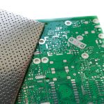
Modern electronic systems are built around Printed Circuit Boards (PCBs). Electronic components mounted on a PCB are electrically interconnected through conductive structures, allowing the board to perform specific functions as part of a complete electronic product.
From simple consumer electronics to sophisticated industrial equipment, PCBs provide the foundation for compact, reliable, and high-performance electronic systems. To understand how a PCB works, it is important to first understand its three fundamental elements: the substrate, conductive pathways, and electronic components.
Every functional element on a PCB has a defined position and electrical purpose. The interaction between these elements determines the board’s electrical performance, mechanical stability, thermal behavior, and overall reliability.
Basic PCB Structure
A typical PCB consists of several interconnected structures. While the exact construction varies according to board type, layer count, material, and application, three fundamental elements are particularly important:
- Conductive pathways
- PCB substrate
- Electronic components
1. Conductive Pathways: The Electrical Framework
The network of conductive pathways is one of the most important parts of a PCB. These structures are commonly referred to as PCB Traces or copper traces.
PCB traces provide electrical connections between components and allow current and electrical signals to travel throughout the circuit.
The geometry of these conductive paths must be carefully controlled during PCB Design. Trace width, spacing, copper thickness, impedance, current capacity, and routing topology can all affect circuit performance.
Copper is the most commonly used conductor because it provides excellent electrical conductivity while remaining relatively cost-effective and compatible with established PCB manufacturing processes.
During PCB Manufacturing, copper layers are patterned through processes such as imaging, etching, plating, and other fabrication steps to create the required circuit geometry.
For multilayer boards, conductive patterns may exist on both outer and inner layers. Vias provide electrical connections between different copper layers, allowing designers to route increasingly complex circuits within a compact footprint.
The resulting routing structure provides several advantages compared with traditional point-to-point wiring:
- More compact circuit construction
- Repeatable electrical connections
- Better organization of signal paths
- Reduced wiring complexity
- Improved manufacturing consistency
- Support for high-density circuit layouts
For high-speed circuits, however, routing is more than simply connecting two components. Engineers must also consider impedance control, signal return paths, crosstalk, electromagnetic compatibility (EMC), and signal integrity.
2. PCB Substrate: Structural and Electrical Foundation
The PCB substrate provides mechanical support and electrical insulation for the conductive layers and components.
The substrate material is selected according to the application’s electrical, mechanical, thermal, and environmental requirements.
FR-4, a glass-fiber-reinforced epoxy laminate, is one of the most widely used PCB substrate materials. It provides a useful combination of mechanical strength, electrical insulation, thermal resistance, dimensional stability, and cost efficiency.
For flexible applications such as wearable electronics, flexible displays, medical devices, and compact products, polyimide is commonly used as a flexible substrate material.
Other specialized PCB materials include:
- High-frequency laminates
- PTFE-based materials
- Metal-core PCB materials
- Ceramic substrates
- High-Tg laminates
- Low-loss dielectric materials
- Flexible and rigid-flex materials
Each material system provides a different balance of electrical performance, thermal characteristics, mechanical properties, and manufacturing cost.
Mechanical Support
One of the primary functions of the substrate is to provide structural stability.
The substrate supports the copper layers and components while maintaining the physical dimensions of the board. Mechanical properties become particularly important in applications exposed to vibration, shock, thermal cycling, bending, or repeated mechanical stress.
Electrical Insulation
The dielectric substrate separates conductive layers and helps prevent unintended electrical connections.
In multilayer PCBs, dielectric materials separate adjacent copper layers while contributing to the controlled impedance of transmission lines.
Thermal Management
PCB materials also influence thermal performance. Although standard FR-4 is widely used, it is not an optimal thermal conductor compared with specialized metal-core or ceramic substrates.
For high-power applications, engineers may consider aluminum PCBs, copper-core structures, ceramic PCBs, or other thermally optimized solutions.
Effective thermal management can help transfer heat away from power components and reduce excessive temperature rise.
3. Electronic Components: Functional Elements of a PCB
Electronic components provide the actual electrical functions of a circuit.
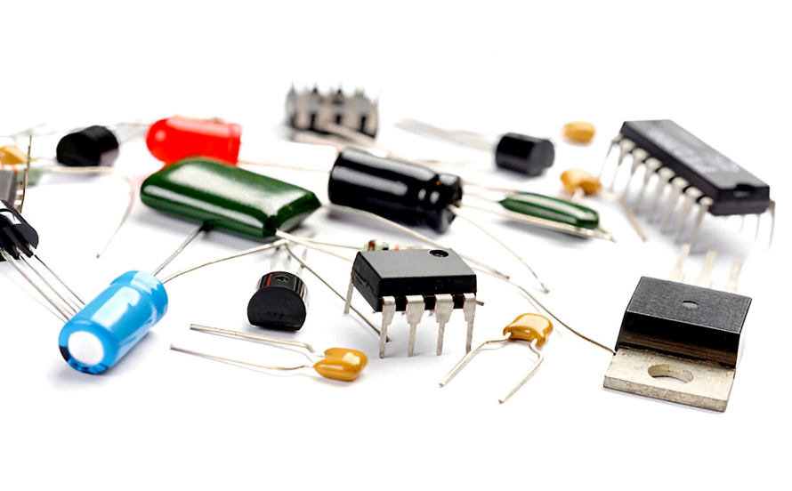
Depending on the application, a PCB may contain processors, memory devices, resistors, capacitors, inductors, sensors, connectors, power-management components, and many other devices.
These components can generally be divided into three broad categories:
- Active components
- Passive components
- Electromechanical components
The correct selection, placement, orientation, and interconnection of these components are essential to the overall performance of the electronic system.
Three Major Categories of PCB Components
1. Active Components
Active Components are electronic devices that generally require an external power source and can control, amplify, switch, or otherwise modify electrical signals.
Common active PCB components include:
- Integrated circuits (ICs)
- Microcontrollers (MCUs)
- Microprocessors (MPUs)
- Transistors
- Diodes
- Operational amplifiers
- Power-management ICs
- RF devices
Integrated circuits can contain thousands, millions, or even billions of transistors depending on their design and application.
A microcontroller, for example, may combine a processor core, memory, timers, communication interfaces, and input/output peripherals in a single package.
The selection of active components directly affects processing capability, power consumption, system functionality, and PCB complexity.
2. Passive Components
Passive Components generally do not provide signal amplification and do not require an external energy source to perform their fundamental electrical functions.
The most common passive components include:
- Resistors
- Capacitors
- Inductors
- Transformers
- Ferrite beads
Each performs a different role in circuit operation.
A resistor can control current and establish voltage relationships. A capacitor can store and release electrical energy, filter unwanted fluctuations, and provide local power decoupling. An inductor can store energy in a magnetic field and oppose rapid changes in current.
For example, decoupling capacitors are commonly positioned close to IC power pins to provide a local source of charge and reduce high-frequency power-supply noise.
Poor passive-component selection or placement can negatively affect power integrity, signal integrity, EMI performance, and overall circuit stability.
3. Electromechanical Components
Electromechanical Components combine electrical and mechanical functions.
Examples include:
- Connectors
- Switches
- Relays
- Buttons
- Sockets
- Potentiometers
- Mechanical sensors
These components often provide the interface between the PCB and the external physical environment.
For example, connectors allow a PCB to communicate with cables, batteries, displays, sensors, or other circuit boards.
Because electromechanical components often experience mechanical forces, their PCB footprints and mounting structures must account for mechanical stress, insertion cycles, vibration, and enclosure constraints.
PCB Components and the Manufacturing Process
The performance of a PCB depends not only on individual components but also on how those components are integrated during PCB Manufacturing.
Several major stages are involved.
1. PCB Design and Layout
The process generally begins with a schematic that defines the electrical relationships between components.
Engineers then use specialized PCB Design Software to convert the schematic into a physical board layout.
The layout determines:
- Component locations
- PCB dimensions
- Copper trace routing
- Via locations
- Layer stackup
- Power and ground planes
- Clearance requirements
- Signal paths
- Mechanical interfaces
For complex boards, designers also need to consider design-for-manufacturing (DFM), thermal management, impedance control, EMI/EMC, and signal integrity.
2. Material Preparation
The PCB substrate is selected according to the electrical and mechanical requirements of the product.
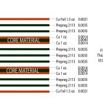
For a multilayer PCB, copper foil, prepreg, core materials, and other dielectric structures are combined to form the required stackup.
The stackup determines the physical relationship between signal layers, power planes, and ground planes.
For high-speed PCB applications, controlled dielectric thickness and material properties are particularly important because they influence transmission-line impedance and signal propagation.
3. Imaging, Etching, and Drilling
During PCB fabrication, circuit patterns are transferred onto copper layers and unwanted copper is removed through controlled etching processes.
Drilling creates through-holes and, depending on the technology, additional structures such as blind or buried vias may be fabricated.
Vias provide electrical connections between different layers and are essential to modern multilayer and HDI PCB designs.
4. PCB Assembly
After PCB fabrication, electronic components must be installed.
The two primary assembly technologies are:
Surface Mount Technology (SMT)
SMT components are mounted directly onto solder pads on the PCB surface.
SMT provides several advantages:
- High component density
- Small component size
- High-speed automated assembly
- Reduced board area
- Efficient mass production
Through-Hole Technology (THT)
Through-hole components use leads that pass through drilled holes in the PCB.
THT components can provide strong mechanical connections and remain useful for connectors, transformers, large capacitors, power components, and applications requiring additional mechanical robustness.
Modern products may use both SMT and THT in the same PCB assembly.
5. Soldering
Depending on the assembly method and product requirements, PCB assemblies may use:
- Reflow soldering
- Wave soldering
- Selective soldering
- Manual soldering
For SMT production, reflow soldering is one of the most widely used processes.
During reflow, solder paste is heated according to a controlled temperature profile so that the solder melts and forms reliable electrical and mechanical connections.
6. Testing and Quality Control
Finished PCB assemblies require inspection and testing to verify that the board meets design and manufacturing requirements.
Common inspection and testing methods include:
- Automated Optical Inspection (AOI)
- Automated X-ray Inspection (AXI)
- In-Circuit Testing (ICT)
- Flying-probe testing
- Functional testing
- Electrical continuity testing
- Insulation resistance testing
- Solder-joint inspection
The appropriate testing strategy depends on board complexity, production volume, reliability requirements, and application.
For high-reliability products, testing and traceability should be integrated throughout the manufacturing process rather than performed only at the final stage.
PCB Design Challenges and Technological Innovation
Designing a basic PCB can already require careful consideration of electrical and mechanical constraints. Designing a complex PCB becomes significantly more challenging when the board contains hundreds or thousands of components, high-speed interfaces, high-current circuits, or RF systems.
Several major challenges must be addressed.
High Component Density
Modern products demand more functionality in smaller spaces.
Engineers increasingly use:
- Fine-pitch components
- HDI technology
- Microvias
- Sequential lamination
- Multilayer PCB structures
- Embedded components
- Miniaturized passive components
These technologies allow more circuits to be integrated into a limited PCB footprint.
Signal Integrity
High-speed interfaces are increasingly common in modern electronic products.
As signal rise times become faster, PCB routing must account for:
- Controlled impedance
- Crosstalk
- Reflections
- Differential-pair matching
- Return-current paths
- Power integrity
- Electromagnetic interference
A PCB that works at low frequencies may require significantly more sophisticated design techniques when operating at high data rates.
Thermal Management
High-performance processors, power-management circuits, LEDs, motors, and power electronics can generate significant heat.
Engineers may need to use:
- Thermal vias
- Copper planes
- Heavier copper
- Metal-core PCBs
- Ceramic substrates
- Heat sinks
- Thermal interface materials
Thermal simulation and temperature testing can help determine whether the PCB can maintain acceptable operating temperatures.
Flexible and Rigid-Flex PCBs
The demand for smaller and more portable products has accelerated the adoption of flexible and rigid-flex PCB technologies.
Flexible PCBs can bend or fold, making them suitable for applications where traditional rigid boards would be difficult to package.
Typical applications include:
- Wearable electronics
- Medical devices
- Cameras
- Mobile electronics
- Automotive systems
- Compact industrial equipment
Miniaturized Components
The continued development of smaller and more capable electronic components is another major driver of PCB miniaturization.
Smaller packages allow engineers to increase functionality without proportionally increasing board dimensions. However, miniaturization also increases placement accuracy requirements, inspection difficulty, routing density, and manufacturing complexity.
Key Factors That Affect PCB Performance
The three basic PCB elements do not operate independently. Their interaction determines the performance of the complete board.
Material Compatibility
PCB laminates, solder materials, component packages, coatings, and other materials must be compatible with the intended manufacturing process and operating environment.
Thermal Performance
The thermal properties of the PCB material, copper distribution, component power dissipation, and cooling structure must be evaluated together.
Signal Integrity
Trace geometry, dielectric properties, stackup, reference planes, vias, and component placement all influence high-speed signal behavior.
Mechanical Reliability
The board must withstand the mechanical conditions expected during manufacturing, transportation, assembly, installation, and operation.
Manufacturing Capability
A PCB design should match the actual capabilities of the manufacturing partner.
Important factors include:
- Minimum trace width and spacing
- Minimum via size
- Registration accuracy
- Layer count
- Copper thickness
- Board thickness
- Surface finish
- Solder mask requirements
- Component placement accuracy
- Testing capability
This is why DFM review should be performed before production whenever possible.
Why Understanding PCB Components Matters
Understanding PCB components is important for engineers, designers, purchasing teams, and manufacturers because each component affects the final product in a different way.
For example, choosing a different capacitor may change the power-supply characteristics. Changing an IC package may alter thermal performance and PCB routing requirements. Changing the substrate may affect impedance, mechanical strength, and heat dissipation.
PCB design is therefore a system-level engineering activity rather than simply the process of drawing copper traces.
A successful board requires coordinated decisions involving:
Components + Materials + Layout + Manufacturing + Assembly + Testing
When these elements are properly integrated, the PCB can achieve the required electrical performance, mechanical reliability, thermal stability, and production consistency.
Kingda PCB Design and Manufacturing Capabilities
Choosing an experienced manufacturing partner is particularly important for complex PCB projects.
Kingda can support PCB projects from fabrication requirements through assembly and testing, helping customers evaluate material selection, layer structures, copper thickness, component placement, manufacturing tolerances, and assembly requirements.
For advanced products, early communication between the design team and manufacturer can help identify potential DFM issues before fabrication begins.
This approach can reduce unnecessary redesigns, improve manufacturing efficiency, and support consistent PCB quality throughout production.
Conclusion
The three fundamental elements of a Printed Circuit Board are the substrate, conductive pathways, and electronic components. Together, they form the physical and electrical foundation of modern electronic systems.
Conductive copper structures provide electrical connections, the substrate supplies mechanical support and electrical insulation, and electronic components perform the functions required by the circuit.
Modern PCB Design has become increasingly sophisticated as products demand smaller dimensions, higher processing performance, faster data transmission, greater power density, and improved reliability. Technologies such as HDI, multilayer construction, flexible circuits, advanced materials, embedded components, and thermal-management structures are helping engineers address these challenges.
At the same time, successful PCB Manufacturing requires precise fabrication, component assembly, soldering, inspection, and electrical testing.
Understanding how PCB components interact with materials, layout, manufacturing processes, and testing is essential for developing reliable electronic products. As electronic technology continues to evolve, engineers who understand these fundamental relationships will be better equipped to design compact, high-performance, and manufacturable PCB solutions.