IC Substrate PCB: PCB Design, PCB Manufacturing, Materials, Types & Applications
Modern electronic devices are becoming smaller, faster, and more computationally powerful every year. Smartphones, laptops, AI accelerators, high-performance servers, automotive electronics, and advanced medical devices increasingly depend on semiconductor packages that contain extremely dense interconnections.
This creates a significant dimensional and electrical gap between the microscopic interconnects of a semiconductor die and the much larger features found on a conventional printed circuit board (PCB).
An IC Substrate PCB, commonly referred to as an IC substrate, helps bridge this gap.
An IC substrate is a thin, high-density interconnection structure positioned between a semiconductor package or die and the system-level PCB. It provides electrical interconnection, mechanical support, power and signal distribution, and—in some package architectures—an important thermal path.
Unlike a conventional PCB designed primarily to mount and interconnect packaged components, an IC substrate is manufactured with much finer features and tighter dimensional tolerances to accommodate advanced semiconductor packaging.
As semiconductor I/O counts continue to increase and package dimensions become smaller, IC substrates have become increasingly important in modern electronics manufacturing.
This guide explains what an IC substrate PCB is, how it differs from a conventional PCB, the major types and materials, the manufacturing process, technical challenges, advantages, applications, and important factors when selecting an IC substrate manufacturing partner.
What Is an IC Substrate PCB?
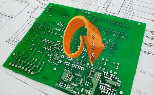
An IC substrate PCB is a high-density interconnection substrate used inside semiconductor packages to connect a semiconductor die or package to the next level of interconnection, typically a motherboard or system PCB.
It acts as an electrical and mechanical interface between the microscopic semiconductor die and the comparatively larger PCB.
A simplified interconnection hierarchy is:
Semiconductor Die → IC Package / IC Substrate → System PCB → Electronic System
The IC substrate can perform several functions:
- Electrical signal routing
- Power and ground distribution
- Mechanical support for the die
- Fan-out of fine-pitch die connections
- Connection to the system PCB
- Thermal management in certain package structures
- Package-level impedance and signal-integrity management
Compared with conventional PCBs, IC substrates typically use much finer line widths, smaller via structures, thinner dielectric layers, tighter registration tolerances, and more advanced substrate materials.
Depending on the package architecture, an IC substrate may contain multiple conductive layers rather than being limited to a single layer.
IC Substrate PCB vs. Conventional PCB
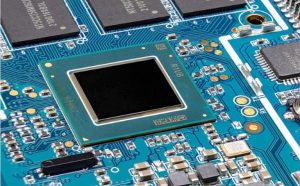
Although IC substrates and conventional PCBs both provide electrical interconnections, they serve different levels of the electronics hierarchy.
| Feature | IC Substrate | Conventional PCB |
|---|---|---|
| Primary Function | Connects semiconductor die/package to the system-level interconnect | Connects packaged electronic components and modules |
| Manufacturing Level | Semiconductor packaging | System-level electronics |
| Feature Size | Extremely fine lines, spaces, pads, and microvias | Generally larger features, depending on PCB technology |
| Dielectric Materials | BT resin, ABF, Ajinomoto build-up films, specialty materials, ceramics, etc. | FR-4, High-Tg FR-4, low-loss laminates, polyimide, metal-core, ceramic, etc. |
| Interconnection | Fine-pitch die/package connections | Component, connector, module, and system connections |
| Manufacturing Tolerance | Extremely tight | Application-dependent |
| Typical Cost per Area | High | Generally lower |
| Typical Applications | CPU, GPU, AI accelerator, memory, SiP, advanced semiconductor packages | Consumer electronics, industrial equipment, automotive systems, networking equipment |
The distinction can be summarized as follows:
IC substrate: package-level interconnection.
Conventional PCB: system-level interconnection.
Both technologies are essential. The IC substrate translates extremely fine semiconductor connections into a format that can ultimately interface with a larger system PCB.
Types of IC Substrate
IC substrates can be classified in several ways, including by package architecture, substrate structure, and die-to-substrate interconnection method.
Common package-related technologies include BGA, CSP, flip-chip packages, chip-scale packages, and system-in-package (SiP) structures.
BGA-Based IC Substrates
Ball Grid Array (BGA) packages use an array of solder balls to establish the connection between the package and the next-level PCB.
The IC substrate routes the fine-pitch connections from the semiconductor die toward the larger BGA ball array.
BGA-based packages can provide:
- High I/O density
- Compact package dimensions
- Efficient electrical interconnection
- Relatively effective thermal paths depending on package construction
BGA is widely used in processors, memory devices, networking components, and other semiconductor packages.
Flip-Chip Substrates
In a flip-chip package, the semiconductor die is mounted with its active surface facing the substrate.
Small solder bumps or copper pillars establish numerous short interconnections between the die and substrate.
This approach offers several important advantages:
- Short electrical paths
- Low parasitic inductance
- High I/O density
- Good electrical performance
- Efficient package-level interconnection
Flip-chip technology is widely used in high-performance processors, GPUs, AI accelerators, networking devices, and other high-I/O semiconductor packages.
Chip-Scale Package (CSP) Substrates
Chip-scale packages are designed to keep the package dimensions relatively close to the dimensions of the semiconductor die.
Because space efficiency is critical, CSP substrates require high-density interconnection and fine-pitch manufacturing.
They are particularly useful in compact consumer electronics and mobile devices.
System-in-Package (SiP) Substrates
SiP technology integrates multiple dies or functional components within a single package.
An SiP substrate may connect:
- Processor dies
- Memory
- RF devices
- Power-management components
- Passive components
- Sensors
This allows multiple functions to be integrated into a compact package.
IC Substrate Interconnection Technologies
Another way to classify IC substrates is by the method used to connect the semiconductor die to the substrate.
Wire Bonding
Wire bonding uses extremely fine metallic wires to connect bonding pads on the semiconductor die to corresponding substrate or package connections.
Common wire materials include gold, copper, and aluminum, depending on the package and process.
Wire bonding is a mature and widely established semiconductor packaging technology.
Its advantages include:
- Mature manufacturing processes
- Relatively low cost
- Broad package compatibility
- Good manufacturing experience and supply-chain availability
However, wire loops introduce longer electrical paths than flip-chip interconnections and may become less attractive for extremely high-I/O or very high-speed applications.
Flip-Chip Bonding
Flip-chip bonding places the die directly over the substrate and uses solder bumps or copper pillars for electrical interconnection.
Because the electrical path is much shorter than a traditional wire bond, flip-chip technology can provide lower parasitic inductance and better high-speed electrical performance.
It is particularly important for:
- CPUs
- GPUs
- AI accelerators
- High-performance computing
- Networking ASICs
- Advanced mobile processors
Materials Used in IC Substrates
Material selection has a major influence on IC substrate performance.
Unlike conventional PCB manufacturing, where FR-4 dominates many applications, IC substrate manufacturing frequently uses specialized dielectric materials designed for fine-line processing, thermal reliability, package-level electrical performance, and high-density interconnection.
BT Resin
BT resin, or bismaleimide-triazine resin, is one of the most widely used materials in IC substrate manufacturing.
It offers a combination of:
- Good thermal resistance
- High mechanical strength
- Electrical insulation
- Dimensional stability
- Suitable package reliability
BT-based substrates are widely used in various semiconductor packages, including BGA and CSP-related applications.
ABF
ABF (Ajinomoto Build-up Film) is a build-up dielectric material widely used in advanced IC substrate applications.
It is particularly important for high-performance semiconductor packages requiring:
- Fine lines and spaces
- Microvias
- Multiple build-up layers
- High-density routing
- High I/O counts
ABF-based build-up substrates are widely associated with advanced processor, GPU, AI accelerator, and high-performance computing packages.
Epoxy-Based Materials
Epoxy resin systems are also used in certain substrate structures where electrical insulation, mechanical stability, manufacturability, and cost efficiency are important.
The exact resin system depends on the package architecture and performance requirements.
Polyimide
Polyimide offers excellent thermal resistance and flexibility.
It is particularly important in flexible circuits and certain specialized semiconductor packaging structures where mechanical flexibility or high-temperature resistance is required.
Ceramic Materials
Ceramic substrates can provide excellent thermal performance and electrical insulation.
Common ceramic materials include:
- Alumina (Al₂O₃)
- Aluminum nitride (AlN)
AlN is particularly attractive for applications requiring high thermal conductivity while maintaining electrical insulation.
Ceramic substrates are used in high-power, RF, LED, automotive, aerospace, and other specialized applications.
Copper
Copper is the primary conductive material used to form electrical interconnections in most IC substrate structures.
Because IC substrates require extremely fine circuitry, copper thickness, plating uniformity, line formation, surface roughness, and dimensional control become particularly important.
How Is an IC Substrate Manufactured?
IC substrate manufacturing is significantly different from conventional PCB Manufacturing.
The process requires highly precise lithography, fine-line formation, thin dielectric layers, microvia fabrication, advanced plating, and extremely accurate layer registration.
A simplified manufacturing workflow may include the following stages.
1. Core and Build-Up Layer Preparation
Depending on the substrate architecture, a core material or supporting substrate is prepared first.
Advanced IC substrates may use sequential build-up structures in which dielectric and copper layers are added progressively.
2. Dielectric Lamination or Film Formation
A dielectric layer is applied to create insulation between conductive layers.
For build-up substrates, materials such as ABF may be laminated and processed to create thin dielectric layers suitable for microvia formation.
3. Microvia Formation
Laser drilling is commonly used to create microvias.
These extremely small vias establish vertical electrical connections between different substrate layers.
Compared with conventional PCB through-holes, IC substrate microvias require much tighter dimensional and positional control.
4. Copper Metallization and Plating
The microvias and conductive structures are metallized and plated with copper.
Uniform plating is essential because variations can affect:
- Electrical resistance
- Via reliability
- Current distribution
- Dimensional accuracy
- Package reliability
5. Fine-Line Circuit Formation
Advanced lithography and patterning processes are used to form extremely fine conductive traces.
The exact process depends on the substrate technology and required line/space dimensions.
6. Build-Up and Layer Registration
Additional dielectric and copper layers are sequentially built up.
Layer-to-layer alignment becomes increasingly important as the substrate becomes more complex.
7. Surface Finishing
Appropriate surface finishes are applied to bonding and package-interconnection areas.
The finish depends on the bonding technology and package requirements.
8. Inspection and Testing
Advanced inspection systems are used to identify defects such as:
- Open circuits
- Short circuits
- Via defects
- Misalignment
- Copper thickness variation
- Surface defects
- Dimensional abnormalities
Electrical testing and package-level reliability testing are also used where required.
Challenges in IC Substrate Manufacturing
IC substrate manufacturing presents challenges that are significantly more demanding than many conventional PCB processes.
1. Extremely Fine Line and Space Requirements
As semiconductor I/O density increases, the substrate must accommodate more electrical connections within a smaller area.
This requires increasingly advanced lithography and fine-line manufacturing technology.
2. Layer Registration
The substrate may contain multiple fine-pitch build-up layers.
Even very small registration errors can affect via capture, electrical connectivity, and package reliability.
Therefore, alignment control is one of the most important manufacturing requirements.
3. Microvia Reliability
Microvias must maintain reliable electrical and mechanical connections throughout manufacturing, assembly, thermal cycling, and product operation.
Potential defects include:
- Voids
- Cracks
- Poor copper deposition
- Incomplete filling
- Delamination
- Interfacial separation
4. Material and Process Control
IC substrate materials can be sensitive to:
- Temperature
- Humidity
- Moisture
- Lamination conditions
- Chemical processing
- Mechanical stress
Manufacturing therefore requires tightly controlled process parameters and environmental conditions.
5. Yield Management
As feature sizes decrease, manufacturing defects can have a greater impact on yield.
A small defect in a fine-pitch substrate can make an entire substrate unusable.
Consequently, inspection, process monitoring, defect analysis, and statistical process control become critical.
Advantages of IC Substrates
Miniaturization
One of the biggest advantages of an IC substrate is its ability to translate extremely fine semiconductor connections into a compact package structure.
Fine lines, microvias, and high-density routing allow more I/O connections to be accommodated in a smaller footprint.
High-Density Interconnection
IC substrates enable dense electrical routing between semiconductor dies and package-level interconnects.
This is essential for modern high-I/O processors and advanced semiconductor packages.
Improved High-Speed Electrical Performance
Short interconnection paths can reduce parasitic inductance and capacitance.
This is especially important for high-speed processors, GPUs, networking ASICs, AI accelerators, and other high-performance devices.
Proper material selection and impedance control are also essential for maintaining signal integrity.
Thermal Management
IC substrate construction can contribute to thermal management, but its exact thermal role depends on the package architecture.
Thermal paths may include:
- Copper structures
- Thermal vias
- Heat spreaders
- Copper pillars
- Package substrates
- Heat sinks
- Direct thermal paths to the package or system board
For very high-power semiconductor devices, the substrate should be considered as part of the complete thermal stack rather than as an isolated heat-dissipation solution.
Package Integration
Advanced IC substrates allow multiple electrical and mechanical functions to be integrated into a relatively compact semiconductor package.
This is one reason they are increasingly important for advanced computing and mobile electronics.
IC Substrate PCB Applications
The growth of AI, high-performance computing, mobile electronics, automotive electronics, and advanced semiconductor packaging continues to increase demand for high-density package substrates.
1. Consumer Electronics
Smartphones, tablets, laptops, wearable devices, and other compact electronics use advanced semiconductor packages that may incorporate IC substrates.
Applications include:
- Mobile processors
- Application processors
- Memory packages
- RF components
- System-in-Package modules
2. AI and High-Performance Computing
AI accelerators, GPUs, CPUs, networking processors, and other high-performance computing devices require extremely high I/O density and high-speed interconnection.
IC substrates provide the fine-pitch electrical interface required between these semiconductor dies and their package-level interconnections.
For advanced AI hardware, substrate design also interacts with power delivery, signal integrity, thermal management, and package size.
3. Automotive Electronics
Automotive semiconductor packages are increasingly required to handle higher computing performance and greater functional integration.
Potential applications include:
- Advanced driver-assistance systems
- Automotive processors
- Radar systems
- Vehicle networking
- Power electronics
- Battery management
- Infotainment systems
Automotive substrate technologies must meet demanding reliability requirements, including thermal cycling and long-term mechanical stability.
4. Medical Electronics
Advanced semiconductor packages are used in medical imaging, monitoring equipment, portable medical electronics, and other specialized systems.
Where IC substrates are used in medical applications, material selection and manufacturing controls must comply with the requirements of the specific medical product.
5. Industrial Electronics
Industrial computing, machine vision, robotics, automation controllers, and intelligent sensors can use semiconductor packages incorporating advanced substrate technologies.
The substrate must provide reliable interconnection under the application’s thermal, mechanical, and environmental conditions.
IC Substrate vs. Interposer vs. Conventional PCB
These three technologies are sometimes confused because they can all provide high-density interconnection.
| Technology | Primary Role | Typical Position |
|---|---|---|
| IC Substrate | Connects semiconductor die/package to system-level interconnection | Inside semiconductor package |
| Interposer | Provides an intermediate high-density interconnection structure between dies and package substrate | Inside advanced package |
| Conventional PCB | Connects packaged components and modules | System level |
In advanced semiconductor packaging, an interposer and IC substrate may be used together.
For example, a high-performance package may include semiconductor dies, an interposer or bridge structure, an IC substrate, and finally the system PCB.
How to Choose an IC Substrate Manufacturer
Selecting an IC substrate manufacturing partner requires significantly different criteria from selecting a conventional PCB manufacturer.
1. Evaluate Fine-Line Manufacturing Capability
Check the manufacturer’s ability to support:
- Fine line/space structures
- Microvias
- Build-up layers
- Fine-pitch pads
- Advanced lithography
- High-precision registration
2. Review Material Experience
Ask whether the manufacturer has experience with the material platform required for your package, such as:
- BT resin
- ABF
- Specialty build-up films
- Polyimide
- Ceramic
- Advanced low-loss materials
3. Evaluate Inspection and Reliability Testing
Important capabilities may include:
- Automated optical inspection
- X-ray inspection
- Cross-section analysis
- Electrical testing
- Microvia reliability testing
- Thermal cycling
- Humidity testing
- Dimensional inspection
4. Examine Engineering and Process Control
Because IC substrates operate at extremely fine dimensions, manufacturing consistency is critical.
Evaluate the manufacturer’s:
- Process control
- Yield management
- Registration control
- Plating uniformity
- Material handling
- Clean manufacturing environment
- Statistical process control
5. Consider Production Capacity
IC substrate projects can involve extremely high volumes and strict yield requirements.
Make sure the supplier can support both prototype validation and the expected production volume.
6. Assess Technical Communication
IC substrate development typically involves close collaboration between semiconductor designers, package engineers, substrate manufacturers, and system PCB engineers.
A manufacturing partner should therefore be able to communicate clearly about material selection, stackup, DFM, tolerances, reliability, and production limitations.
IC Substrate PCB and PCB Design Considerations
Although IC substrate design occurs at the package level, it is closely connected to system-level PCB Design.
Engineers should consider:
- Package pin assignment
- BGA escape routing
- Power distribution
- Ground structures
- Controlled impedance
- Signal integrity
- Power integrity
- Thermal paths
- Via structures
- Package-to-PCB transition
- Mechanical constraints
A well-designed IC substrate can simplify the transition between extremely fine semiconductor connections and the larger routing geometry of the system PCB.
Kingda and Advanced PCB Manufacturing
For projects involving advanced package-to-board interconnections, the manufacturing requirements should be defined at the beginning of the product-development cycle.
Kingda can support PCB-related projects involving high-density interconnection, multilayer structures, controlled impedance, HDI technologies, and advanced PCB Manufacturing requirements according to the project’s specifications.
For semiconductor packaging projects, customers should first determine whether they require a conventional PCB, HDI PCB, IC substrate, interposer, or a hybrid package architecture. These technologies involve different materials, equipment, manufacturing tolerances, and qualification requirements.
Frequently Asked Questions
What is an IC substrate PCB?
An IC substrate is a high-density interconnection structure used between a semiconductor die/package and a system-level PCB.
It provides electrical routing, mechanical support, and package-level interconnection while translating fine-pitch semiconductor connections into a format suitable for the next level of the electronic system.
Is an IC substrate the same as a PCB?
Not exactly.
An IC substrate is technically a substrate used in semiconductor packaging, while a conventional PCB is generally a system-level interconnection board.
Although both use conductive and dielectric structures, their feature sizes, materials, manufacturing processes, tolerances, and applications are different.
What materials are used in IC substrates?
Common materials include BT resin, ABF build-up films, epoxy-based dielectric systems, polyimide, ceramic materials, and copper.
The appropriate material depends on package architecture, electrical requirements, thermal requirements, manufacturing process, and reliability targets.
Are IC substrates single-layer or multilayer?
IC substrates can be single-layer or multilayer, depending on their architecture.
Advanced semiconductor packages commonly use multilayer build-up structures to accommodate high I/O density and complex power and signal routing.
What is the difference between an IC substrate and an HDI PCB?
Both can use fine lines and microvias, but they operate at different levels.
An HDI PCB is generally a system-level PCB technology designed to increase routing density.
An IC substrate is designed specifically for semiconductor packaging and normally requires significantly tighter feature dimensions and manufacturing tolerances.
Why are IC substrates important for AI processors?
AI processors and accelerators can contain very high numbers of I/O connections and require high-bandwidth communication, substantial power delivery, and effective thermal management.
IC substrates provide the high-density package-level interconnection required to connect these semiconductor devices to the larger electronic system.
Conclusion
IC substrates have become an increasingly important part of modern semiconductor packaging.
They bridge the substantial physical and electrical gap between microscopic semiconductor dies and system-level PCBs. By providing fine-pitch routing, high-density interconnection, mechanical support, and package-level electrical and thermal functions, IC substrates enable advanced processors and compact electronic systems to operate efficiently.
Unlike conventional PCBs, IC substrates are manufactured using highly specialized materials and processes, including BT resin, ABF build-up films, microvias, fine-line lithography, advanced copper plating, and precise layer registration.
Their importance is particularly evident in AI accelerators, CPUs, GPUs, smartphones, networking equipment, automotive electronics, high-performance computing, and advanced medical and industrial systems.
As semiconductor devices continue to increase in I/O density, processing capability, and power consumption, IC substrate technology will remain closely connected to the development of advanced packaging and system-level PCB Design.
For manufacturers and engineering teams, the key is to select the appropriate substrate architecture, materials, interconnection technology, and manufacturing process according to the semiconductor package and final system requirements.