6-Layer PCB Stackup: PCB Design, PCB Manufacturing & Layer Configuration Guide
As modern electronics continue to demand higher operating frequencies, faster data rates, greater functionality, and smaller form factors, Multilayer PCB technology has become a critical enabler of advanced electronic products. This is particularly important when designers need to accommodate complex circuitry within a limited physical space.
Among common multilayer configurations, the 6-Layer PCB provides a practical balance between routing density, signal integrity, power distribution, electromagnetic compatibility (EMC), and manufacturing complexity. It is widely considered for high-speed digital systems, mixed-signal electronics, communication equipment, industrial controls, medical devices, and other applications where a four-layer board may no longer provide sufficient design flexibility.
A six-layer board contains six copper layers separated by dielectric materials. With careful planning, these layers can be assigned to signal routing, ground references, power distribution, and shielding functions. However, simply adding two more signal layers to a four-layer design does not automatically produce a better PCB. The stackup must be engineered around the electrical, mechanical, thermal, and manufacturing requirements of the product.
Because six-layer boards generally involve greater fabrication complexity and material usage than four-layer PCBs, strategic PCB Design and manufacturability planning are essential for obtaining the expected performance without unnecessarily increasing cost.
What Is a 6-Layer PCB Stackup?
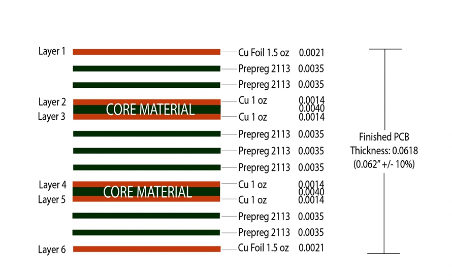
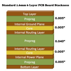
A 6-Layer PCB Stackup is the specific arrangement of six conductive copper layers and the dielectric materials separating them. Depending on the construction method, the dielectric materials may include cores and prepregs with different thicknesses and electrical properties.
A typical six-layer PCB can be organized as:
| Layer | Typical Function |
|---|---|
| Layer 1 | Signal / Component Layer |
| Layer 2 | Ground Plane |
| Layer 3 | Power Plane / Signal |
| Layer 4 | Power / Signal / Ground |
| Layer 5 | Signal / Ground Plane |
| Layer 6 | Signal / Ground / Component Layer |
The exact assignment is not universal. A stackup should be selected according to routing requirements, impedance targets, component placement, power architecture, via strategy, EMI/EMC requirements, and the capabilities of the selected PCB manufacturer.
Why Choose a 6-Layer PCB?
There are several situations in which a six-layer configuration can provide meaningful advantages over a four-layer board.
1. Limited Routing Space
Insufficient routing space is one of the most straightforward reasons to consider a six-layer PCB. However, designers should not simply copy a four-layer design and add two additional signal layers.
A better approach is to reconsider the complete board architecture. The additional layers can be used strategically to create dedicated signal paths, power distribution areas, and reference planes. This may allow the final board to become smaller while supporting more circuitry.
2. Blind and Buried Vias
Blind and buried vias can be implemented in four-layer boards, but their benefits often become more significant as layer count and routing density increase.
A six-layer stackup provides additional internal routing resources that can make Blind Vias and Buried Vias useful for connecting selected layers without occupying routing space across the entire board thickness.
However, these structures also increase PCB Manufacturing complexity and cost. They should therefore be introduced only when they solve a genuine routing, size, or electrical problem.
3. High-Speed and Mixed-Signal Designs
Six-layer PCBs can provide multiple signal layers with dedicated reference planes, making them suitable for high-speed digital and mixed-signal applications.
A well-designed stackup can help control:
- Characteristic impedance
- Return-current paths
- Crosstalk
- Electromagnetic interference (EMI)
- Power integrity
- Signal integrity
- Ground bounce
- Differential-pair performance
For mixed-signal systems, sensitive analog circuitry can also be physically separated from noisy digital or switching-power sections. However, simply assigning different layers to analog and digital signals does not guarantee good EMC performance. Grounding, return paths, component placement, routing, filtering, and power distribution must all be considered together.
Functions of Each Layer in a 6-Layer PCB Stackup
The following is a representative six-layer configuration. Actual stackups may differ depending on the application and fabrication process.
Layer 1: Top Copper Layer
The top copper layer is normally the primary component-placement and signal-routing layer.
Surface-mounted components are typically placed on this side because it provides convenient access for automated assembly. High-speed signal traces can also be routed on this layer when a closely spaced reference plane is available underneath.
For high-speed PCB Design, the distance between the top signal layer and its reference plane is extremely important. This dielectric thickness affects characteristic impedance and electromagnetic coupling.
The top layer is commonly used for:
- High-speed signal routing
- Differential pairs
- Component connections
- Critical clock signals
- Short power connections
- Local copper pours
In many designs, unnecessary power routing on the top layer should be minimized because it can consume valuable routing space and complicate signal integrity.
Layer 2: Ground Plane
The second copper layer is frequently assigned as a continuous ground plane.
A solid ground plane provides a low-impedance return path for high-frequency signals and serves as an electrical reference for traces routed on Layer 1.
This configuration is particularly useful for controlled-impedance designs because the geometry between Layer 1 and Layer 2 can be used to calculate and control microstrip impedance.
A continuous ground plane can also help reduce electromagnetic radiation and crosstalk, provided that it is not unnecessarily fragmented by routing or inappropriate plane cuts.
For many six-layer designs, keeping Layer 2 as continuous as possible is more valuable than using it as another general-purpose signal layer.
Layer 3: Power Plane or Signal Layer
Layer 3 can serve different functions depending on the design architecture.
A common configuration uses this layer for power distribution. Multiple voltage domains may be implemented using appropriately divided copper regions.
Another option is to use Layer 3 as a signal-routing layer when the power architecture does not require a dedicated plane.
However, power-plane segmentation should be carefully planned. Improper splits can force high-speed return currents to take longer paths, potentially increasing loop area and EMI.
For this reason, power-plane design should always be evaluated together with the signal layers immediately above and below it.
Layer 3 Dielectric
The dielectric material between Layer 3 and the next copper layer provides electrical isolation and contributes to the mechanical structure of the PCB.
Its thickness, dielectric constant (Dk), and dissipation factor (Df) can influence high-speed electrical performance.
In cost-sensitive designs, prepreg may be used where its electrical uniformity requirements are less demanding. For controlled-impedance applications, however, the manufacturer must account for the actual material system and finished stackup rather than relying only on nominal material specifications.
Layer 4: Ground, Power, or Signal Layer
Layer 4 is one of the most flexible layers in a six-layer PCB.
Depending on the application, it may be assigned as:
Ground Layer
Layer 4 can provide an additional ground reference, particularly when another internal signal layer requires strong electromagnetic isolation.
A ground plane between signal layers can reduce coupling and provide a controlled return-current path.
Signal Layer
Layer 4 can also be used for signal routing when the design has a high I/O count or requires additional routing capacity.
However, high-speed signals should not be routed on an internal layer without considering their reference plane. A signal layer should have a clearly defined adjacent reference plane so that its return current can follow a predictable path.
Power Layer
For systems containing multiple voltage rails, Layer 4 can be used for power distribution.
This approach can provide dedicated copper regions for different voltage domains while preserving other layers for signals and ground.
The final decision should be based on the actual power architecture rather than simply following a generic stackup template.
Layer 4 Dielectric
The dielectric layer surrounding Layer 4 contributes to both electrical isolation and overall board thickness.
Its thickness and material properties affect the spacing between signal layers and reference planes. Therefore, changing this dielectric thickness during PCB Manufacturing can alter impedance values.
This is particularly important when a PCB has strict controlled-impedance requirements.
For production, the PCB designer and manufacturer should agree on the complete stackup before fabrication so that the impedance calculations correspond to the actual material construction.
Layer 5: Signal or Ground Layer
Layer 5 is commonly used as either a signal layer or a ground/reference plane.
Signal Layer
When a signal layer needs additional EMI protection, placing it between ground-reference layers can create a favorable electromagnetic environment.
For example, a configuration in which Layer 4 and Layer 6 act as reference planes can help confine electromagnetic fields around Layer 5.
However, the effectiveness depends on the continuity of the reference planes and the geometry of the stackup.
When high-speed signals are routed on Layer 5, impedance must be calculated using the actual distance to its reference plane, dielectric constant, copper thickness, trace width, and surrounding geometry.
Ground Layer
Layer 5 can alternatively function as a ground plane when the bottom side of the PCB is intended for high-speed routing or component placement.
A dedicated ground plane provides a reference for the bottom signal layer and can help establish a predictable return path.
Layer 5 Dielectric
The dielectric between Layer 5 and Layer 6 is especially important when Layer 6 contains high-speed traces.
Its thickness and dielectric properties directly affect the impedance of bottom-layer transmission lines.
For this reason, the top and bottom dielectric structures may be designed similarly in a symmetrical stackup. However, identical construction is not mandatory; the correct configuration depends on the required electrical and mechanical characteristics.
Layer 6: Bottom Copper Layer
The bottom copper layer can be used for either signal routing, component placement, or ground, depending on the PCB architecture.
Bottom Layer as a Ground Plane
When Layer 5 contains sensitive or high-speed signals that require strong reference-plane control, Layer 6 can be used as a ground plane.
This configuration can provide electromagnetic shielding and a stable return-current path.
However, using the bottom layer entirely as ground may limit component placement and bottom-side routing.
Bottom Layer as a Signal Layer
The bottom layer can also be used for signal routing and component placement.
This is particularly useful when the board requires additional routing density or when components need to be installed on both sides.
For high-speed signals, however, designers should ensure that the bottom traces have an adjacent and continuous reference plane. Via transitions should also be minimized where practical because every transition can introduce additional parasitic inductance and discontinuity.
Symmetrical vs. Asymmetrical 6-Layer Stackups
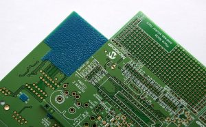
Multilayer PCBs can be constructed using either symmetrical or asymmetrical stackups.
Symmetrical Stackup
A symmetrical six-layer stackup generally attempts to balance the copper and dielectric structures around the center of the board.
For example:
| Layer | Function |
|---|---|
| L1 | Signal |
| L2 | Ground |
| L3 | Power |
| L4 | Power / Ground |
| L5 | Ground |
| L6 | Signal |
The exact material thicknesses and copper weights can be balanced to reduce mechanical stress.
Symmetrical constructions are often attractive because balanced structures can help reduce warpage and improve manufacturing consistency during lamination.
Asymmetrical Stackup
An asymmetrical stackup intentionally uses different layer assignments, dielectric thicknesses, or copper distributions.
This can be useful when the electrical requirements of the top and bottom sides are substantially different.
For example, one side may contain high-density components and high-speed routing while the other side primarily handles power distribution or low-speed signals.
Although asymmetrical structures are possible, they require careful manufacturing analysis. Significant differences in copper distribution and dielectric construction can affect lamination behavior, board flatness, impedance, and dimensional stability.
Therefore, the stackup should be reviewed with the PCB fabricator before production.
Typical 6-Layer PCB Stackup Examples
There is no single stackup that is optimal for every six-layer PCB. Several configurations are possible.
Example 1: General-Purpose Six-Layer Stackup
| Layer | Function |
|---|---|
| L1 | Signal / Components |
| L2 | Ground |
| L3 | Signal / Power |
| L4 | Power / Signal |
| L5 | Ground |
| L6 | Signal / Components |
This arrangement provides dedicated ground references while retaining multiple routing layers.
Example 2: High-Speed 6-Layer Stackup
| Layer | Function |
|---|---|
| L1 | High-Speed Signal |
| L2 | Solid Ground |
| L3 | Power |
| L4 | High-Speed / Differential Signal |
| L5 | Solid Ground |
| L6 | Signal / Components |
This type of architecture can provide controlled reference planes for both outer and inner signal layers.
Example 3: Mixed-Signal Stackup
| Layer | Function |
|---|---|
| L1 | Components / Critical Signals |
| L2 | Ground |
| L3 | Digital / Power |
| L4 | Analog / Digital Signals |
| L5 | Ground |
| L6 | Low-Speed Signals / Components |
The actual analog and digital partitioning should be determined by circuit topology and current return paths rather than treating the ground plane as an arbitrary barrier.
6-Layer PCB Stackup and Signal Integrity
One of the main reasons to select a six-layer PCB is improved control of signal integrity.
At high frequencies, PCB traces behave as transmission lines rather than simple wires. Their electrical behavior depends on:
- Trace width
- Copper thickness
- Dielectric thickness
- Dielectric constant
- Reference-plane distance
- Trace geometry
- Differential-pair spacing
- Via structure
- Connector characteristics
A carefully engineered stackup allows designers to calculate controlled impedance before routing begins.
For example, a high-speed trace on Layer 1 can use Layer 2 as its reference plane. Similarly, an internal signal layer can be designed with a nearby ground plane to create a controlled transmission-line structure.
This is one reason why PCB Stackup Design should be completed before detailed routing.
6-Layer PCB Stackup for EMI and EMC Control
A properly designed six-layer stackup can contribute significantly to EMI and EMC performance.
The basic principles include:
- Keep high-speed signal layers close to continuous reference planes.
- Minimize signal-loop area.
- Avoid unnecessary gaps or splits in reference planes.
- Provide short and low-inductance return paths.
- Use ground vias appropriately around critical structures.
- Separate noisy power circuits from sensitive analog circuits.
- Minimize unnecessary layer transitions.
- Control differential-pair geometry and symmetry.
A ground plane is not automatically an EMI shield simply because it exists. Its effectiveness depends on continuity, current return paths, via structures, component placement, and the overall enclosure and grounding strategy.
Manufacturing Considerations for 6-Layer PCBs
Moving from four layers to six layers increases manufacturing complexity. Therefore, PCB Manufacturing considerations should be incorporated into the design from the beginning.
Important factors include:
Material Selection
The dielectric system should be selected according to frequency, loss requirements, thermal performance, and cost.
For high-speed applications, Dk and Df become increasingly important.
Copper Thickness
Copper weight affects current-carrying capability, thermal performance, trace width, impedance, and manufacturability.
The copper distribution across layers should also be considered because large differences in copper density can contribute to fabrication issues.
Via Technology
Through vias are usually the most economical option. Blind and buried vias can provide routing advantages but generally increase manufacturing complexity.
Microvias may also be considered for high-density designs when appropriate.
Controlled Impedance
If the design includes high-speed interfaces such as USB, PCIe, Ethernet, DDR, RF, or other high-frequency interfaces, impedance requirements should be communicated to the manufacturer.
The manufacturer should calculate the finished stackup based on the actual laminate and copper construction.
Lamination and Board Flatness
Six-layer PCBs require multiple copper and dielectric layers to be laminated together. The balance of copper distribution, dielectric thickness, and material properties can affect board flatness and dimensional stability.
A well-balanced stackup can make production more predictable.
How to Optimize a 6-Layer PCB Stackup
A reliable six-layer design should be developed systematically rather than selecting a generic stackup and routing immediately.
Step 1: Define Electrical Requirements
Identify:
- Maximum operating frequency
- Data rates
- Controlled-impedance requirements
- Differential interfaces
- Power domains
- Analog and digital sections
- EMI/EMC requirements
Step 2: Determine Layer Functions
Assign each copper layer a primary purpose before routing begins.
Avoid treating every layer as a general-purpose routing layer.
Step 3: Establish Reference Planes
High-speed signals should have nearby, continuous reference planes.
Step 4: Calculate Impedance
Use the actual dielectric thickness, Dk, copper thickness, trace width, and geometry to determine impedance.
Step 5: Review Via Strategy
Determine whether through vias are sufficient or whether blind, buried, or microvia structures are justified.
Step 6: Perform DFM Review
Check the stackup against the manufacturer’s capabilities, including minimum trace/space, hole sizes, aspect ratio, copper thickness, registration, and lamination requirements.
Step 7: Validate Signal and Power Integrity
For demanding designs, simulation can be used to evaluate impedance, crosstalk, return loss, insertion loss, power integrity, and other high-speed effects.
6-Layer PCB vs. 4-Layer PCB
| Feature | 4-Layer PCB | 6-Layer PCB |
|---|---|---|
| Routing Capacity | Moderate | Higher |
| Layer Count | 4 | 6 |
| Ground/Power Planning | More limited | More flexible |
| High-Speed Design | Suitable for moderate complexity | More routing/reference options |
| Mixed-Signal Design | Possible | Greater architectural flexibility |
| EMI/EMC Control | Good with proper design | More opportunities for dedicated references |
| Via Options | Mainly through vias | Greater potential for advanced via structures |
| Manufacturing Cost | Generally lower | Generally higher |
| Design Complexity | Lower | Higher |
The additional two layers do not automatically guarantee better electrical performance. Their value comes from how effectively they are used to manage routing, references, power distribution, and signal integrity.
Common 6-Layer PCB Design Mistakes
Several mistakes can reduce the benefits of a six-layer configuration.
Using Every Layer for Routing
A PCB with six copper layers does not necessarily need six routing layers. Dedicated ground and power structures can be more valuable than additional unrestricted routing space.
Breaking Up Reference Planes
Splitting a ground plane beneath a high-speed signal can force return current to detour, increasing loop area and potentially causing EMI problems.
Ignoring Dielectric Thickness
The distance between a trace and its reference plane strongly affects impedance. Changing the dielectric structure without recalculating impedance can cause the finished PCB to deviate from the intended electrical characteristics.
Adding Advanced Vias Without Need
Blind and buried vias can solve routing problems, but they also increase fabrication complexity and cost. They should be justified by board density, form factor, or electrical requirements.
Designing Without Manufacturer Input
A theoretically excellent stackup may not be economical or manufacturable using every PCB fabricator’s process.
Early communication between the designer and manufacturer can prevent unnecessary redesigns.
Applications of 6-Layer PCBs
Six-layer PCBs are commonly considered for applications requiring greater routing density and electrical control, including:
- High-speed computing equipment
- Networking and telecommunications
- Industrial automation
- Medical electronics
- Automotive electronics
- Consumer electronics
- Embedded systems
- Data acquisition systems
- Power management equipment
- IoT gateways
- Communication modules
- Mixed-signal instrumentation
The appropriate stackup depends on the application’s electrical and mechanical requirements rather than simply the product category.
Kingda 6-Layer PCB Manufacturing Support
For a six-layer PCB, successful production depends on more than simply fabricating six copper layers. The PCB Manufacturing process must accurately reproduce the specified stackup, dielectric structure, copper thickness, via construction, impedance characteristics, and dimensional requirements.
Kingda can support six-layer PCB projects from design review and DFM analysis through PCB fabrication and assembly. For high-density and high-speed designs, the manufacturing review can focus on stackup feasibility, impedance control, via structures, copper distribution, registration, and other critical production factors.
By involving the manufacturer early in the design process, engineers can identify manufacturability issues before prototype fabrication and reduce the risk of costly redesigns.
Conclusion
A well-engineered 6-Layer PCB provides significantly more architectural flexibility than a four-layer board. The additional copper layers can be strategically assigned to signal routing, power distribution, ground references, and EMI/EMC control, making six-layer configurations particularly useful for high-speed and mixed-signal electronics.
However, the number of layers alone does not determine PCB performance. The quality of the PCB Design, stackup geometry, reference-plane continuity, impedance control, via strategy, power distribution, and manufacturing process all contribute to the final result.
For demanding applications, the most effective approach is to define the electrical requirements first, establish a manufacturable stackup, calculate controlled impedance, optimize return-current paths, and then complete detailed routing. Working closely with an experienced PCB Manufacturing partner such as Kingda can further improve manufacturability and production consistency while helping control unnecessary fabrication costs.