Multilayer PCB: PCB Design, PCB Manufacturing, Structure & Applications
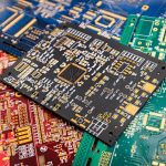
Multilayer printed circuit boards (PCBs) have become essential components in modern electronics, automation, communication systems, and industrial equipment. The growing demand for compact, high-performance, reliable, and energy-efficient electronic products has driven the development of increasingly sophisticated Multilayer PCB technology.
Modern electronic devices are expected to deliver more functions while occupying less physical space. As component density, processing capability, and data rates continue to increase, a two-layer PCB may no longer provide sufficient routing space or electrical performance. Multilayer PCB technology addresses this challenge by allowing designers to distribute power, ground, and signal networks across multiple conductive layers within a compact board structure.
A multilayer PCB is particularly valuable when an electronic product requires high routing density, controlled impedance, improved signal integrity, efficient power distribution, and better electromagnetic compatibility (EMC).
This guide explains what a multilayer PCB is, its structure, manufacturing process, applications, advantages and disadvantages, and the differences between multilayer and double-sided PCBs.
What Is a Multilayer PCB?
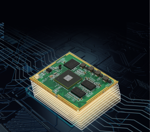
A Multilayer PCB is a printed circuit board containing more than two conductive copper layers separated by dielectric insulating materials.
Unlike a conventional double-sided PCB, which has copper layers on the top and bottom surfaces, a multilayer board incorporates additional copper layers inside the PCB structure. These internal layers can be assigned to signal routing, power distribution, ground planes, or other specialized functions.
A typical multilayer PCB may contain:
- Signal layers
- Ground planes
- Power planes
- Core materials
- Prepreg dielectric layers
- Through vias
- Blind vias
- Buried vias
- Solder mask
- Surface finish
- Silkscreen
The exact number and arrangement of these layers depend on the electrical requirements, mechanical dimensions, operating environment, and manufacturing process.
Multilayer PCBs are widely used in:
- Consumer electronics
- Automotive electronics
- Industrial automation
- Medical equipment
- Telecommunications
- Computers and servers
- Aerospace electronics
- Defense systems
- Test and measurement equipment
- Networking equipment
- IoT devices
The primary advantage is that complex circuits can be integrated into a relatively compact physical area without continuously increasing the PCB’s length and width.
Multilayer PCB Structure
Understanding the structure of a multilayer PCB is essential before discussing its manufacturing process.
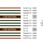
1. PCB Layer Identification
The defining characteristic of a multilayer PCB is its multiple conductive layers.
Each layer performs a specific function within the overall circuit architecture. The major structural materials include copper layers, core materials, and prepreg.
Depending on the design, conductive layers may function as:
- Signal layers for routing electrical signals
- Ground layers for providing reference and return-current paths
- Power layers for distributing supply voltages
The designer determines the layer functions during the PCB Design stage.
A well-engineered stackup is particularly important for high-speed designs because layer spacing, dielectric properties, copper thickness, and reference-plane configuration directly affect impedance and signal integrity.
2. Vias and Interconnections
Vias provide electrical connections between different copper layers.
Common via structures include:
- Through vias — extend through the entire PCB
- Blind vias — connect an external layer to one or more internal layers
- Buried vias — connect internal layers without reaching the external surfaces
- Microvias — typically used in high-density interconnect applications
Vias allow signals and power networks to transition between layers while maintaining electrical continuity.
However, vias are not electrically invisible. At high frequencies, via structures introduce parasitic inductance and capacitance and can create impedance discontinuities. Therefore, via placement and geometry should be considered carefully in high-speed PCB Design.
3. PCB Stackup
The stackup defines the order and thickness of the conductive and dielectric layers.
For example, a seven-layer PCB might theoretically contain a combination of:
- Top signal layer
- Power layer
- Signal layer
- Ground layer
- Signal layer
- Power layer
- Bottom signal layer
The exact configuration varies according to the application.
A properly engineered PCB Stackup can provide:
- Controlled impedance
- Short signal-return paths
- Improved power integrity
- Better signal integrity
- Reduced crosstalk
- Improved EMI/EMC performance
- Greater routing flexibility
An unsuitable stackup can make routing difficult and may negatively affect electrical performance, manufacturability, and cost.
4. Input and Output Connections
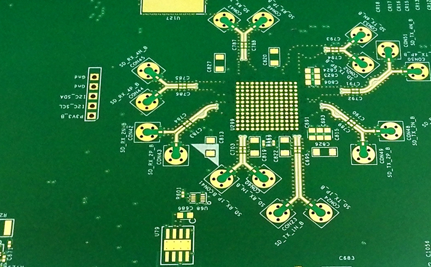
Every electronic circuit has defined input and output requirements. In a multilayer PCB, connectors, component pads, vias, and traces must be arranged so that signals can move efficiently between external interfaces and internal circuitry.
High-speed input/output interfaces require special attention to:
- Trace impedance
- Differential-pair geometry
- Return paths
- Connector transitions
- Via placement
- Ground continuity
- Crosstalk
For complex systems, feedback and internal communication between functional blocks must also be carefully managed.
Multilayer PCB Manufacturing Process
The PCB Manufacturing process for a multilayer board is considerably more complex than that of a single-sided or basic double-sided PCB.
Each manufacturing stage must maintain dimensional accuracy, layer registration, electrical continuity, and material integrity.
1. PCB Design and Internal Layer Preparation
Every PCB project begins with a design.
During the design stage, engineers define:
- Layer count
- PCB dimensions
- Component footprints
- Trace widths and spacing
- Via structures
- Copper thickness
- Material selection
- Stackup
- Impedance requirements
- Power and ground distribution
- Mechanical constraints
- Manufacturing tolerances
The completed design data is then converted into manufacturing files, such as Gerber or other production data formats, depending on the manufacturer’s workflow.
For complex multilayer designs, DFM and DFMA (Design for Manufacturing and Assembly) reviews are important before fabrication begins.
Applicable IPC standards should also be considered when selecting materials, fabrication processes, and acceptance criteria.
For example, material specifications and PCB construction requirements should be matched to the intended application rather than selecting materials solely on the basis of cost.
2. Inner-Layer Fabrication
The internal copper layers are fabricated before the final multilayer lamination process.
Typically, the process includes:
- Copper-clad laminate preparation
- Cleaning and surface treatment
- Photoresist application
- Image transfer
- Exposure
- Development
- Copper etching
- Inspection
- Inner-layer quality verification
The resulting inner-layer patterns form the internal signal, ground, and power networks.
Because these layers will eventually be enclosed inside the PCB, defects such as shorts, opens, insufficient copper, or incorrect patterns can be difficult to repair after lamination. Therefore, inner-layer inspection is an important quality-control step.
3. Layer Stacking and Lamination
After the inner layers are prepared, the individual cores, copper foils, and prepreg materials are arranged according to the specified stackup.
The materials are then laminated under controlled temperature and pressure.
During lamination, the prepreg softens and bonds the layers together, creating a rigid multilayer structure.
Lamination must be carefully controlled because excessive or insufficient pressure, temperature variations, material differences, or layer misalignment can lead to:
- Delamination
- Voids
- Layer shifting
- Resin-related defects
- Dimensional instability
- Warpage
Thermal expansion is also important because different materials expand at different rates.
For demanding applications, the selection of laminate material and thermal characteristics should be considered during the initial PCB Design stage.
4. Drilling and Plating
After lamination, holes are drilled according to the manufacturing data.
These holes may be used for:
- Component leads
- Through vias
- Mechanical mounting
- Electrical interconnection
The drilled holes are subsequently cleaned and prepared for plating.
Copper plating is used to create electrical continuity through the hole walls and connect the relevant conductive layers.
For multilayer boards, drilling accuracy is particularly important because a small registration error can prevent a via from properly connecting its intended layers.
Advanced multilayer designs may use laser drilling for microvias, especially when HDI technology is required.
5. Outer-Layer Preparation
After drilling and plating, the external copper layers are patterned.
The manufacturing process typically includes imaging, resist processing, copper pattern formation, etching, and inspection.
The goal is to create accurate external traces, pads, copper areas, and other conductive features according to the PCB design.
Manufacturing tolerances must be carefully controlled because fine-pitch components and high-density routing require precise trace and pad dimensions.
6. Solder Mask and Surface Finish
A solder mask is applied to protect exposed copper and reduce the risk of unintended solder bridging during assembly.
The solder mask also provides electrical insulation and protects the PCB surface from environmental exposure.
A silkscreen layer can then be applied to identify:
- Component reference designators
- Polarity markings
- Connector locations
- Test points
- Manufacturing information
The final PCB surface finish is selected according to the electrical, mechanical, environmental, and assembly requirements.
Common surface finishes include:
- HASL
- Lead-free HASL
- ENIG
- OSP
- Immersion Tin
- Immersion Silver
- ENEPIG
The correct surface finish depends on factors such as component pitch, shelf life, solderability, contact requirements, and application environment.
7. Final Inspection and Electrical Testing
Quality control is performed throughout the multilayer PCB Manufacturing process.
Typical inspection and testing methods may include:
- Automated Optical Inspection (AOI)
- Inner-layer inspection
- Dimensional inspection
- Solder mask inspection
- X-ray inspection
- Electrical continuity testing
- Isolation testing
- Controlled-impedance testing
- Microsection analysis when required
Electrical testing verifies that intended conductive paths are continuous and that unintended connections are not present.
For high-reliability applications, additional inspection and testing requirements may apply according to the applicable industry standards and customer specifications.
Applications of Multilayer PCBs
Multilayer PCBs are used across almost every major electronics sector because they combine routing density, compact construction, and design flexibility.
1. Consumer Electronics
Modern smartphones, tablets, laptops, home appliances, entertainment systems, and other consumer devices often require multilayer PCB technology.
As products become thinner while incorporating more processors, memory, wireless interfaces, sensors, and power-management circuits, multilayer construction provides additional routing capacity without requiring a proportionally larger board.
2. Industrial Automation
Industrial control systems often operate in environments where reliability, electrical noise immunity, and mechanical durability are important.
Multilayer PCBs can integrate control circuits, communication interfaces, sensor systems, power-management circuits, and processing units into compact assemblies.
Applications include:
- PLC systems
- Motor controllers
- Robotics
- Industrial sensors
- Machine-vision equipment
- Factory automation systems
3. Smartwatches and Wearable Electronics
Wearable devices require extremely compact electronics.
A multilayer PCB allows designers to place more circuitry into a small physical area while keeping interconnections short.
This is especially important for smartwatches and other wearable products that integrate processors, wireless communication, displays, sensors, battery management, and health-monitoring functions.
4. Medical and Diagnostic Equipment
Medical electronics often require high reliability, compact construction, and stable electrical performance.
Multilayer PCBs are used in various medical and diagnostic systems, including:
- Patient monitoring equipment
- Imaging systems
- Diagnostic instruments
- Portable medical devices
- Laboratory equipment
- Medical control systems
For safety-critical medical electronics, material selection, manufacturing controls, inspection, traceability, and applicable regulatory requirements must be considered carefully.
5. Automotive Electronics
Modern vehicles contain increasingly complex electronic systems.
Multilayer PCBs can be found in:
- Advanced driver assistance systems
- Infotainment systems
- Engine control electronics
- Battery management systems
- Vehicle networking
- Instrument clusters
- Automotive sensors
Automotive applications may require enhanced thermal, vibration, humidity, and reliability performance.
6. Telecommunications and Networking
High-speed communication equipment depends heavily on carefully engineered multilayer PCBs.
Routers, switches, wireless equipment, optical communication systems, and network infrastructure may require multiple signal layers, controlled impedance, dedicated reference planes, and carefully designed power distribution.
7. Aerospace and Defense
Aerospace and defense systems often require compact, lightweight, reliable, and highly controlled electronic assemblies.
Multilayer PCB technology allows complex electronic functions to be integrated within constrained mechanical envelopes.
Applications include communication equipment, navigation systems, radar-related electronics, control systems, and instrumentation.
Multilayer PCB vs. Double-Sided PCB
A double-sided PCB contains copper circuitry on both sides of a dielectric substrate. A multilayer PCB contains more than two conductive layers, including internal copper layers.
The key differences are summarized below:
| Feature | Double-Sided PCB | Multilayer PCB |
|---|---|---|
| Conductive Layers | 2 | More than 2 |
| Routing Capacity | Moderate | High |
| Circuit Complexity | Low to moderate | Moderate to very high |
| Power/Ground Planning | More limited | More flexible |
| Signal Integrity Options | Limited compared with multilayer designs | Greater flexibility |
| Controlled Impedance | Possible | More design options |
| Manufacturing Complexity | Lower | Higher |
| Typical Cost | Lower | Higher |
| Board Density | Moderate | High |
| Typical Applications | Prototypes, controls, lighting, simple electronics | Smartphones, computers, networking, medical, automotive, aerospace |
Double-Sided PCB
A double-sided PCB generally consists of a substrate with copper circuitry on both sides.
It is suitable for applications where circuit complexity and routing requirements are relatively moderate.
Typical applications include:
- Industrial controllers
- LED lighting
- Simple consumer electronics
- Prototypes
- Hobby electronics
- Basic instrumentation
Multilayer PCB
A multilayer PCB adds internal copper layers, significantly increasing routing capacity.
The internal layers can be dedicated to power and ground, allowing the external layers to focus on component connections and signal routing.
This makes multilayer boards more suitable for high-density and high-performance electronics.
Advantages of Multilayer PCBs
1. Higher Circuit Density
Multiple conductive layers allow more circuitry to be incorporated into the same physical footprint.
This is one of the primary reasons multilayer PCBs are widely used in compact electronic products.
2. Compact Product Design
Because circuits can be distributed vertically through multiple layers, designers can reduce the required PCB footprint.
This is especially valuable for portable and wearable electronics.
3. Better Signal Integrity
A carefully engineered stackup can place high-speed signal layers close to continuous reference planes.
This can reduce loop area and improve return-current behavior.
4. Improved Power Distribution
Dedicated power and ground structures provide greater flexibility for distributing multiple voltage rails.
A solid ground plane can also provide a stable electrical reference for high-speed signals.
5. Greater EMI/EMC Control
Additional ground planes and carefully arranged signal layers can help control electromagnetic coupling.
However, good EMI/EMC performance still depends on the complete system design, including routing, grounding, filtering, shielding, component placement, and enclosure design.
6. Greater Design Flexibility
Multilayer construction allows designers to separate different circuit functions across multiple layers.
For example, a board can include dedicated areas for high-speed signals, analog circuits, power distribution, and ground references.
7. Reduced Interconnection Length
A properly designed multilayer PCB can reduce the physical distance between interconnected components.
Shorter interconnections can help reduce parasitic effects and improve overall electrical performance.
Disadvantages of Multilayer PCBs
Despite their advantages, multilayer PCBs also introduce several challenges.
1. Higher Manufacturing Cost
Additional copper layers, dielectric materials, lamination processes, drilling, plating, inspection, and testing increase manufacturing costs compared with simpler PCBs.
2. Greater Design Complexity
Designing a multilayer board requires careful consideration of:
- Stackup
- Signal integrity
- Power integrity
- Impedance
- Thermal management
- EMI/EMC
- Via structures
- Manufacturability
3. More Difficult Repair
Internal copper layers are inaccessible after final lamination. Therefore, diagnosing and repairing internal-layer defects is generally more difficult than repairing visible external traces.
4. Longer Production Time
Multilayer fabrication involves more manufacturing stages and tighter process control.
Consequently, prototype and production lead times may be longer than those of simpler two-layer boards.
5. Thermal and Mechanical Challenges
Multiple materials and lamination cycles introduce thermal and mechanical stresses.
Poorly balanced copper distribution or unsuitable material combinations can contribute to warpage, delamination, or dimensional problems.
How to Choose the Right Multilayer PCB
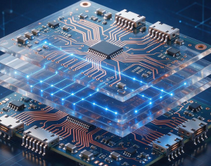
The appropriate layer count should be determined by the actual electrical and mechanical requirements rather than simply selecting a higher layer count.
Consider the following factors:
Circuit Complexity
Determine whether the circuit can be routed effectively using two or four layers. If routing becomes excessively congested, additional layers may be justified.
Signal Speed
High-speed interfaces often require carefully controlled impedance and dedicated reference planes.
Power Requirements
Products containing multiple voltage domains may benefit from dedicated power and ground structures.
Board Size
If the PCB must fit within a compact mechanical enclosure, additional layers may allow the board footprint to remain small.
EMI/EMC Requirements
Products operating in electrically noisy environments may benefit from carefully planned ground and signal layers.
Manufacturing Cost
More layers generally increase fabrication cost. The target layer count should therefore provide the required electrical performance without unnecessary complexity.
Manufacturer Capability
Before finalizing the stackup, confirm that the selected PCB Manufacturing partner can reliably produce the required layer count, material system, copper thickness, via structures, impedance tolerances, and minimum feature sizes.
Multilayer PCB Design Best Practices
For reliable and manufacturable multilayer PCB designs, engineers should:
- Define the stackup before detailed routing.
- Use continuous reference planes for critical high-speed signals.
- Minimize unnecessary signal-layer transitions.
- Keep high-speed return paths short and continuous.
- Separate noisy power circuits from sensitive analog circuitry.
- Use controlled impedance where required.
- Select materials according to frequency and thermal requirements.
- Balance copper distribution where practical.
- Consider DFM early in the design process.
- Work with the PCB manufacturer before finalizing complex stackups.
A strong PCB Design process considers electrical performance and manufacturing feasibility simultaneously.
Kingda Multilayer PCB Manufacturing
Multilayer PCB fabrication requires precise control of layer registration, material thickness, copper distribution, lamination, drilling, plating, surface treatment, and electrical testing.
Kingda can support multilayer PCB projects from design and manufacturability review through fabrication and assembly. For demanding multilayer designs, the manufacturing review can focus on stackup feasibility, material selection, controlled impedance, via structures, copper thickness, dimensional tolerances, and inspection requirements.
Early cooperation between the engineering team and the manufacturer can help identify potential manufacturing issues before production, reducing redesigns and improving overall project efficiency.
Conclusion
Multilayer PCB technology has become fundamental to modern electronic product development because it enables complex circuits to be integrated into compact, reliable, and high-performance assemblies.
Compared with double-sided PCBs, multilayer boards provide substantially greater routing capacity and more flexible power, ground, and signal-layer configurations. These characteristics make them suitable for consumer electronics, automotive systems, industrial automation, telecommunications, medical equipment, aerospace, defense, and other demanding applications.
However, multilayer PCB technology also introduces higher manufacturing costs, greater design complexity, longer production processes, and more demanding quality-control requirements.
The key to a successful multilayer PCB is not simply increasing the number of layers. Engineers must optimize the stackup, signal-return paths, impedance, power distribution, thermal characteristics, via structures, and manufacturability according to the application’s actual requirements.
By combining a carefully engineered PCB Design with a capable PCB Manufacturing partner such as Kingda, manufacturers can achieve a practical balance between electrical performance, reliability, compactness, and production cost.