Through-Hole PCB Assembly: PCB Design, PCB Manufacturing & THT Guide
Through-hole assembly may appear to be a straightforward PCB assembly method, but producing reliable, long-lasting solder joints requires precise component placement, controlled soldering processes, and experienced manufacturing techniques. Although Surface Mount Technology (SMT) has become dominant in modern electronics, Through-Hole PCB Assembly remains an important manufacturing method, particularly for applications that require strong mechanical connections, high reliability, and resistance to harsh operating conditions.
Through-hole technology is widely used for connectors, transformers, relays, power components, large capacitors, switches, and other components that must withstand mechanical or thermal stress.
This guide explains what through-hole PCB assembly is, what THT means, the main types of through-hole components, the complete assembly process, its advantages and disadvantages, and how to choose a reliable through-hole PCB assembly manufacturer.
What Is Through-Hole PCB Assembly?
Through-Hole PCB Assembly is a PCB assembly process in which component leads are inserted through drilled holes in a printed circuit board and then soldered to conductive pads, typically on the opposite side of the board.
The process is also commonly referred to as Through-Hole Technology (THT) or Through-Hole Assembly.
Unlike SMT components, which are mounted directly onto PCB surface pads, through-hole components use leads that pass through the PCB substrate. The leads can then be soldered using manual soldering, wave soldering, selective soldering, or other appropriate processes.
Common through-hole components include:
- Transformers
- Large capacitors
- Power resistors
- Relays
- Connectors
- Switches
- Terminal blocks
- Inductors
- Large diodes
- Power semiconductors
- Mechanically reinforced components
Through-hole assembly generally requires more PCB area than SMT because the component bodies and drilled holes occupy more space. However, the mechanical strength of a properly soldered through-hole connection can be highly valuable in products exposed to vibration, shock, high current, or repeated mechanical insertion.
Modern products often combine SMT and THT rather than choosing only one technology. SMT can be used for high-density electronic circuits, while THT components can be added where mechanical strength or power-handling requirements justify them.
What Does THT Mean in Through-Hole PCB Assembly?
THT stands for Through-Hole Technology.
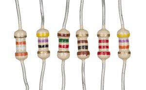
In THT assembly, component leads are inserted into plated or non-plated holes designed for the component. When the holes are plated through, the copper plating creates an electrical connection between the component lead and the PCB’s conductive layers.
After insertion, the leads are soldered to the corresponding pads.
Depending on the production requirements, THT components can be installed through:
- Manual insertion
- Automated insertion
- Manual soldering
- Wave soldering
- Selective soldering
THT is one of the earliest component mounting technologies used in PCB manufacturing. Despite the widespread adoption of SMT, THT remains important for components that require high mechanical strength, large lead spacing, high current capability, or specialized package structures.
It is also useful for prototypes, low-volume production, repair, maintenance, and products containing large or mechanically stressed components.
Types of THT Components Used in Through-Hole PCB Assembly
Through-hole components can generally be classified according to their lead configuration and component geometry.
Axial Through-Hole Components
Axial components have leads extending from opposite ends of the component body.
The component is normally positioned horizontally across the PCB, with one lead inserted into a hole at each end.
Typical examples include:
- Axial resistors
- Certain inductors
- Some diodes
- Fuses
Axial components are relatively easy to place and can be installed manually or by specialized automated insertion equipment.
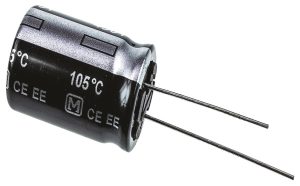
Radial Through-Hole Components
Radial components have their leads extending from the same side of the component body.
They can generally be mounted vertically or horizontally depending on the component design and PCB requirements.
Common examples include:
- Electrolytic capacitors
- Ceramic capacitors
- LEDs
- Some inductors
- Certain connectors
- Power components
Radial components are frequently used where the component body must remain close to the PCB or where the design requires a compact lead arrangement.
Through-Hole PCB Assembly Process
A reliable PCB Assembly process requires accurate documentation, component verification, controlled insertion, proper soldering, inspection, and testing.
A typical THT assembly workflow includes the following stages.
1. Manufacturing Data Verification
The customer first provides the complete manufacturing package to the PCB assembly manufacturer.
Depending on the project, this package may include:
- Bill of Materials (BOM)
- Gerber files
- PCB fabrication drawings
- Assembly drawings
- Pick-and-place files, if applicable
- Schematic files
- THT assembly instructions
- Component specifications
- Test requirements
- Special manufacturing instructions
The manufacturer reviews the documentation to verify component quantities, reference designators, PCB specifications, polarity requirements, hole sizes, component orientations, and assembly requirements.
A detailed engineering review helps identify inconsistencies before production begins.
2. Component Preparation
Before insertion, components are checked against the BOM and assembly documentation.
The manufacturer may verify:
- Part number
- Manufacturer
- Package type
- Value
- Tolerance
- Polarity
- Lead configuration
- Quantity
- Component condition
Components may need to be formed, cut, trimmed, or prepared for automated insertion depending on the assembly method.
3. Through-Hole Component Placement
Once the manufacturing data and components have been verified, THT components are inserted into the PCB.
There are two main approaches.
Manual Component Insertion
Operators manually insert components according to the assembly drawing and work instructions.
Manual insertion is particularly practical for:
- Prototypes
- Low-volume production
- Mixed-technology assemblies
- Large components
- Unusual component packages
- Frequently changing designs
Experienced operators are important because incorrect orientation, polarity, or component location can cause electrical or functional problems.
Automated Component Insertion
For suitable components and production volumes, automated insertion equipment can place through-hole components more quickly and consistently.
Automated insertion may use component coordinates and programmed placement information.
Compared with manual insertion, automated equipment can improve production speed and repeatability when the component packaging and PCB design are compatible with the machine.
4. THT Component Soldering
After component insertion, the leads must be securely soldered to the PCB.
The main THT soldering methods include manual soldering, wave soldering, and selective soldering.
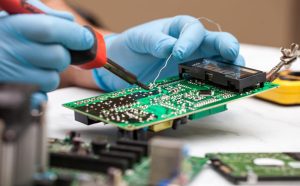
Manual Soldering
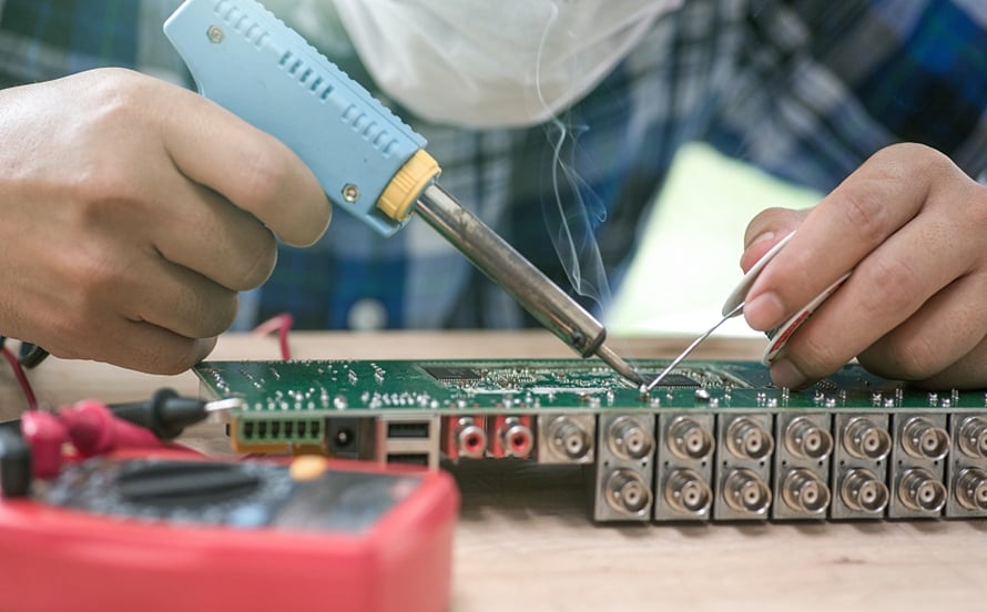
Manual soldering uses a soldering iron or other controlled soldering equipment to create individual solder joints.
The operator applies solder to the component lead and PCB pad while controlling temperature and solder quantity.
Manual soldering is useful for:
- Prototypes
- Small production batches
- Repair
- Rework
- Special components
- Components that cannot pass through automated soldering processes
The quality of manual soldering depends heavily on operator training, soldering temperature, contact time, solder quantity, flux compatibility, and inspection procedures.
Wave Soldering
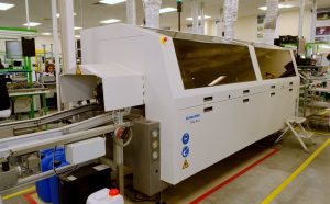
Wave soldering is one of the most common automated soldering methods for THT PCB assembly.
During wave soldering, the PCB passes over a controlled bath of molten solder. A solder wave contacts the exposed component leads and PCB pads on the solder side, forming multiple solder joints simultaneously.
A typical wave soldering process includes:
- Flux application
- Preheating
- Contact with molten solder
- Cooling
- Inspection
Flux is applied to promote solder wetting and remove or reduce surface oxides. The PCB is then preheated before passing through the solder wave.
Wave soldering is particularly suitable for boards containing many compatible through-hole components.
Selective Soldering
Selective soldering is useful when a PCB contains both SMT and THT components and only specific through-hole locations require soldering.
Instead of exposing the entire underside of the PCB to a large solder wave, a controlled solder nozzle selectively applies molten solder to designated locations.
This can reduce thermal exposure to nearby components and is especially useful for mixed-technology PCBs.
5. PCB Cleaning
After soldering, PCB cleaning may be required depending on the flux chemistry and product requirements.
Not every PCB requires aggressive cleaning. The cleaning method should be selected according to the type of flux used, component sensitivity, PCB materials, and cleanliness requirements.
Possible cleaning methods include:
- Deionized water cleaning
- Aqueous cleaning
- Solvent-based cleaning
- Specialized PCB cleaning systems
The objective is to remove unwanted flux residues, contaminants, and other process residues when required.
For sensitive electronics, manufacturers may perform ionic contamination or cleanliness testing to verify that the board meets the specified requirements.
6. Quality Inspection and Testing
Quality inspection is an essential part of PCB Manufacturing and PCB assembly.
A THT PCBA may undergo several inspection and testing methods depending on the product requirements.
Visual Inspection
Operators inspect:
- Component placement
- Component orientation
- Polarity
- Solder joints
- Missing components
- Damaged components
- Solder bridges
- Insufficient solder
- Excessive solder
- Mechanical defects
AOI
Automated Optical Inspection (AOI) uses cameras and image-processing algorithms to identify assembly defects.
AOI can help detect:
- Missing components
- Incorrect orientation
- Incorrect component placement
- Solder-related defects
- Polarity errors
- Visible assembly defects
AOI is particularly valuable in mixed SMT/THT production lines.
ICT
In-Circuit Testing (ICT) checks electrical characteristics and circuit nodes using dedicated test fixtures and probes.
Depending on the test system and PCB design, ICT can detect issues such as:
- Open circuits
- Short circuits
- Incorrect component values
- Certain component failures
- Connectivity problems
Functional Testing
Functional testing evaluates whether the completed PCBA performs its intended electrical functions.
The board may be powered under controlled conditions and tested using the same or simulated inputs and outputs that it will encounter in the final product.
Functional testing is especially important for complex industrial, automotive, medical, telecommunications, and power electronics assemblies.
X-Ray Inspection
X-ray inspection can be useful when solder joints or internal structures cannot be adequately evaluated through visual inspection.
It may be used for:
- Hidden solder joints
- Complex packages
- Certain connectors
- Voids
- Internal structural defects
The appropriate inspection method depends on the component package and product requirements.
7. Packaging and Shipping
After inspection and testing, qualified PCB assemblies are packaged for delivery.
Packaging may include:
- ESD-safe bags
- Protective trays
- Anti-static materials
- Bubble protection
- Moisture-control packaging where required
- Product labels
- Barcode labels
- Shipping documentation
For sensitive electronic assemblies, packaging must protect the PCBA from electrostatic discharge, moisture, mechanical shock, and contamination during transportation.
If an order contains multiple product configurations, assemblies can also be separated into individual kits or production lots.
Advantages of Through-Hole PCB Assembly
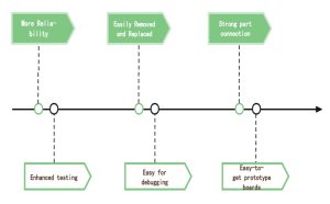
Although SMT provides higher component density and automated placement capabilities, THT remains valuable for many applications.
Strong Mechanical Connections
One of the primary advantages of THT is mechanical strength.
Because component leads pass through the PCB, the connection provides mechanical anchoring in addition to the electrical connection.
This makes THT particularly useful for:
- Connectors
- Switches
- Transformers
- Relays
- Large capacitors
- Power components
- Components exposed to vibration or mechanical stress
Suitable for Harsh Environments
Through-hole components can be advantageous in products that experience mechanical shock, vibration, or repeated connector insertion.
This is one reason THT continues to appear in industrial, automotive, aerospace, defense, and power electronics applications.
Easier Manual Rework
Through-hole components are often easier to access and replace during repair or rework.
Technicians can typically remove the solder and extract the component using conventional rework tools, although multilayer boards with plated-through holes may require careful thermal management to avoid pad or barrel damage.
Good Prototyping Capability
THT components are widely used in prototypes because their larger physical size and accessible leads make them relatively easy to inspect and rework.
Engineers can manually replace components during development without requiring a complete automated assembly process.
Suitable for Large Components
Some high-power or mechanically demanding components are difficult or impractical to mount exclusively using SMT.
THT provides a practical solution for components such as:
- Large connectors
- Transformers
- Relays
- Terminal blocks
- High-power components
- Large capacitors
Flexible Assembly Options
THT assembly can use manual insertion, automated insertion, wave soldering, selective soldering, or combinations of these methods.
This flexibility makes it suitable for prototypes as well as certain high-volume manufacturing environments.
Disadvantages of Through-Hole PCB Assembly
Despite its advantages, THT also has several limitations compared with SMT.
Higher Space Requirements
Through-hole components require drilled holes and generally occupy more PCB area.
The component bodies can also be larger than equivalent SMT packages.
This makes THT less suitable for extremely compact electronics where component density is a major design priority.
More Complex PCB Routing
Each through-hole requires physical space and may pass through multiple PCB layers.
On a multilayer PCB, a plated through-hole can consume routing space on inner layers and may interfere with high-density routing.
Designers therefore need to consider hole placement early in the PCB Design process.
Lower Component Density
SMT components can be manufactured in very small packages and placed closely together.
THT components generally require larger spacing because of their lead dimensions and drilling requirements.
As a result, THT is usually less suitable for miniaturized high-density electronic products.
More Drilling Requirements
THT assembly requires component holes to be drilled during PCB fabrication.
Additional drilling increases manufacturing complexity and can affect PCB cost, routing space, and production yield.
Longer Assembly Time for Manual Production
Manual insertion and soldering can take significantly longer than automated SMT placement.
The production time becomes especially significant when a board contains a large number of THT components.
Higher Labor Requirements
Manual THT assembly requires trained operators to identify components, check orientation, insert leads, trim leads when necessary, and solder or inspect the joints.
Human errors can occur if appropriate work instructions and inspection systems are not implemented.
However, automated insertion and automated soldering can significantly reduce these risks.
THT vs. SMT PCB Assembly
THT and SMT are complementary technologies rather than mutually exclusive alternatives.
| Feature | THT Assembly | SMT Assembly |
|---|---|---|
| Component mounting | Leads pass through PCB holes | Components mount on surface pads |
| Component size | Generally larger | Can be extremely compact |
| Component density | Lower | Higher |
| Mechanical strength | Generally strong | Depends on package and solder-joint design |
| Drilling | Required for through-hole components | Generally not required for component mounting |
| Automation | Available for suitable components | Highly automated |
| Prototyping | Convenient for many designs | Also suitable, especially with modern prototyping services |
| Rework | Often accessible | Requires specialized tools for small packages |
| Typical applications | Connectors, transformers, relays, power components | High-density digital, consumer, communication, and compact electronics |
| Best use case | Mechanical strength and larger components | Miniaturization and high component density |
Many modern products use mixed-technology PCB assembly, combining SMT and THT on the same board.
For example, small resistors, capacitors, ICs, and processors may use SMT, while connectors, transformers, and large power components use THT.
PCB Design Considerations for THT Assembly
Successful THT production begins with appropriate PCB design.
Hole Size
The finished hole diameter must accommodate the component lead while maintaining appropriate solderability and mechanical requirements.
Designers should consider:
- Component lead diameter
- Hole tolerance
- Plating thickness
- Finished hole size
- Assembly tolerance
Pad Size
Through-hole pad dimensions influence solderability and mechanical reliability.
The pad should provide enough copper area to form a reliable solder joint without unnecessarily consuming routing space.
Component Spacing
Adequate spacing is necessary for:
- Automated insertion
- Manual assembly
- Wave soldering
- Inspection
- Rework
- Thermal management
Component Orientation
Component orientation should be standardized wherever practical.
Consistent orientation makes assembly and inspection easier and reduces the possibility of polarity or placement errors.
Thermal Relief
Thermal relief structures may be required when through-hole pads connect directly to large copper planes.
Without appropriate thermal design, excessive heat may be required to achieve proper solder wetting.
Solder-Side Clearance
Designers should verify that adequate clearance exists around THT solder joints, especially when the board contains dense copper planes or nearby SMT components.
Wave and Selective Soldering Compatibility
If wave soldering will be used, the PCB layout should account for:
- Component orientation
- Solder flow
- Shadowing
- Pad geometry
- Component spacing
- Thermal exposure
- Solder bridging risk
Design-for-assembly should therefore be incorporated into the PCB layout before fabrication.
How to Choose a Through-Hole PCB Assembly Manufacturer
Choosing a qualified Through-Hole PCB Assembly Manufacturer is important for achieving consistent solder quality and production reliability.
Consider the following factors.
Manufacturing Experience
Check whether the manufacturer has experience with:
- THT assembly
- Mixed SMT/THT assembly
- Manual insertion
- Automated insertion
- Wave soldering
- Selective soldering
- Manual rework
Quality Certifications
Depending on the application, relevant certifications may include:
- ISO 9001
- ISO 14001
- IATF 16949
- ISO 13485
- UL-related requirements
- IPC standards
The appropriate certification should match the product’s industry and regulatory requirements.
Inspection and Testing Capabilities
A qualified assembly partner should provide appropriate inspection and testing capabilities, such as:
- AOI
- ICT
- Functional testing
- X-ray inspection where applicable
- Visual inspection
- Electrical testing
- First Article Inspection
Component Sourcing
Reliable component procurement is essential for THT assembly.
The manufacturer should be able to verify:
- Manufacturer part numbers
- Component authenticity
- Package type
- Availability
- Lead time
- Substitution requirements
- Obsolescence risks
Production Flexibility
A capable manufacturer should be able to support different production volumes, from prototypes and small batches to larger production runs.
DFM and DFA Support
The manufacturer should review the PCB and assembly data before production.
A DFM/DFA review can identify potential issues involving:
- Hole sizes
- Pad dimensions
- Component spacing
- Lead clearance
- Wave soldering compatibility
- Component orientation
- Assembly sequence
- Test access
Through-Hole PCB Assembly Services from Kingda
Kingda can support customers requiring Through-Hole PCB Assembly, SMT assembly, and mixed-technology PCBA manufacturing.
For THT projects, the manufacturing process can be organized around the customer’s BOM, Gerber files, assembly drawings, schematics, component specifications, testing requirements, and production quantities.
The engineering team can review the design for manufacturability and assembly considerations before production begins. Depending on the project, the manufacturing process can incorporate manual insertion, automated assembly, wave soldering, selective soldering, inspection, electrical testing, and functional testing.
For products requiring both high-density SMT and mechanically robust THT components, a mixed-technology assembly approach can combine the advantages of both technologies on a single PCBA.
Conclusion
Through-Hole PCB Assembly remains an important PCB assembly technology despite the widespread adoption of SMT. Its ability to provide mechanically robust component connections makes it particularly useful for connectors, transformers, relays, power components, terminal blocks, and products exposed to vibration, mechanical stress, or demanding operating environments.
THT assembly typically involves manufacturing data verification, component preparation, through-hole insertion, soldering, cleaning when required, inspection, electrical testing, and packaging.
Compared with SMT, THT generally requires more PCB space, additional drilling, and potentially more labor. However, it offers strong mechanical connections, good accessibility for rework, and excellent compatibility with many large or mechanically stressed components.
For modern electronics, the most practical solution is often not choosing between THT and SMT, but using the appropriate technology for each component. A well-designed mixed SMT/THT assembly can combine high component density with the mechanical strength and reliability required by demanding applications.