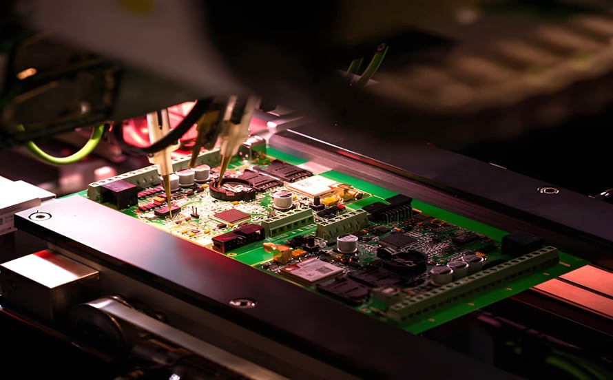
PCB ICT Testing: PCB Design, PCB Manufacturing & In-Circuit Test Process
As printed circuit boards (PCBs) become increasingly complex, manufacturers are integrating more components and interconnections into smaller board areas. This growing design density makes reliable PCB testing essential for maintaining product quality, electrical performance, and manufacturing consistency.
In-Circuit Testing (ICT) is one of the most widely used methods for verifying assembled PCBs. Unlike functional testing, which primarily evaluates whether a completed circuit performs its intended function, ICT examines individual components, electrical connections, and selected circuit nodes on the board.
A properly implemented ICT process can detect manufacturing defects early, verify component placement and orientation, identify soldering problems, and provide detailed information for troubleshooting and process improvement.
This article explores the PCB ICT Testing process in detail, including its preparation, fixture development, programming, test execution, troubleshooting, data analysis, advantages, and limitations.
What Is PCB ICT Testing?
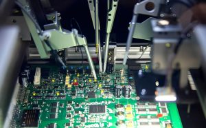
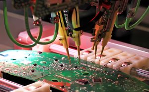
PCB ICT Testing is an automated electrical testing method that uses test probes to contact designated test points or component terminals on an assembled PCB. The system applies electrical signals and measures parameters such as continuity, resistance, capacitance, voltage, current, and selected logic responses.
ICT systems commonly use either a dedicated bed-of-nails fixture or a flying-probe tester, depending on production volume, board design, and testing requirements.
The primary objectives of ICT include:
- Detecting manufacturing defects at an early stage
- Verifying component values and placement
- Checking component orientation and polarity
- Detecting open circuits and short circuits
- Identifying soldering defects
- Measuring electrical parameters against predefined limits
- Verifying selected circuit connections
- Improving overall PCB assembly quality
- Providing diagnostic information for failed boards
ICT is typically performed after PCB Assembly and soldering. Testing at this stage allows manufacturers to identify defects before the product proceeds to functional testing or final system integration.
By detecting manufacturing and assembly problems early, ICT can reduce unnecessary rework, prevent defective boards from moving further through production, and provide valuable feedback for manufacturing process improvement.
Key Components of an ICT System
A complete ICT system consists of several hardware and software components working together.
Test Fixture
The test fixture provides the physical interface between the tester and the PCB.
For traditional ICT, a bed-of-nails fixture contains multiple spring-loaded probes, often called pogo pins, positioned to contact designated test points on the PCB.
The fixture must provide reliable and repeatable electrical contact during every test cycle. Its mechanical accuracy is particularly important because even a small positioning error can cause intermittent contact or inaccurate measurements.
Dedicated ICT Test Program
The ICT system requires a dedicated test program that defines how the PCB should be tested.
The program typically specifies:
- Test nodes
- Test sequence
- Measurement methods
- Component limits
- Acceptable tolerances
- Electrical conditions
- Pass/fail criteria
- Diagnostic information
The test program is generally developed from PCB design data, schematics, component information, netlists, and manufacturing requirements.
Test Equipment and Peripheral Devices
An ICT system may include various measurement and control devices, such as:
- Programmable power supplies
- Digital multimeters
- Signal generators
- Switching matrices
- Measurement instruments
- Logic measurement hardware
- Control computers
- Data acquisition systems
Specialized software coordinates test execution, data collection, pass/fail decisions, reporting, troubleshooting, and statistical analysis.
PCB ICT Testing Process
The effectiveness of PCB ICT Testing depends heavily on proper preparation. ICT should not be considered an isolated inspection step; instead, it should be integrated into the PCB Design, assembly, manufacturing, and quality-control workflow.
The following steps describe a typical ICT process.
1. Design for Test (DFT) Preparation
Effective ICT begins during the PCB Design stage.
Engineers should incorporate suitable test points for power, ground, signals, component nodes, and critical nets. Test points must be positioned so that probes can make reliable contact without interfering with components, traces, or mechanical structures.
Important DFT considerations include:
- Test-point accessibility
- Probe size
- Probe pitch
- Probe clearance
- Test-point pad dimensions
- Board-edge clearance
- Component height restrictions
- Ground and power test points
- Signal test points
- Test-point density
A well-designed DFT strategy can significantly improve test coverage and reduce the complexity and cost of ICT fixture development.
2. ICT Fixture Development
After the PCB layout has been finalized, the test fixture can be designed according to the board geometry, test-point locations, netlist, and manufacturing data.
For a traditional bed-of-nails ICT system, the fixture is customized to match the PCB.
The fixture must ensure:
- Accurate PCB positioning
- Reliable probe contact
- Proper board alignment
- Adequate mechanical support
- Safe application of test signals
- Repeatable test conditions
Before entering mass production, the fixture should be verified to ensure that all required electrical and mechanical functions operate correctly.
For lower-volume production or frequently changing PCB designs, flying-probe testing can eliminate the need for a dedicated mechanical fixture, although test-cycle time is generally longer.
3. ICT Test Program Development
The ICT test program defines how each PCB will be evaluated.
Individual test nodes are assigned unique identifiers so that the test system can accurately locate and evaluate them.
Depending on the PCB design, the program may include:
- Continuity tests
- Resistance measurements
- Capacitance measurements
- Inductance measurements
- Diode tests
- Transistor checks
- Component-value verification
- Polarity verification
- Short-circuit detection
- Open-circuit detection
- Voltage measurements
- Logic-level tests
Test limits are normally established according to component specifications, circuit requirements, manufacturing tolerances, and engineering documentation.
For more complex boards, engineers may also need to consider test access limitations caused by high-density routing, BGA packages, fine-pitch components, and multilayer structures.
4. Unpowered and Powered Testing
ICT generally begins with tests that can be safely performed while the PCB is unpowered.
This stage can identify problems such as:
- Short circuits
- Open circuits
- Incorrect resistance
- Incorrect capacitance
- Incorrect component values
- Component polarity errors
- Incorrect connections
- Some soldering defects
After appropriate unpowered tests have been completed, the board can be powered under controlled conditions when powered testing is required.
This staged approach helps reduce the risk of damaging components and allows basic manufacturing defects to be identified before more advanced electrical tests are performed.
5. Test Execution and Pass/Fail Criteria
Once the fixture and ICT program are ready, testing becomes part of the production workflow.
The operator places the assembled PCB into the fixture and verifies its orientation and alignment.
The tester then executes the predefined test sequence automatically.
Measurement results are compared against predetermined limits.
A PCB is considered to have passed ICT when all required measurements fall within their specified limits and no critical fault is detected.
If one or more measurements fall outside the permitted range, the board is classified as failed and sent for further diagnosis.
6. Troubleshooting and Repair
Failed PCBs should undergo failure analysis to determine the actual cause of the problem.
Because ICT evaluates individual components and circuit nodes, it can provide valuable diagnostic information for identifying potential failures.
Common causes may include:
- Incorrect component placement
- Wrong component value
- Reversed polarity
- Missing components
- Solder bridges
- Insufficient solder
- Open solder joints
- Damaged components
- Incorrect PCB connections
- Manufacturing defects
After the defect has been repaired, the PCB should be tested again to confirm that the problem has been successfully resolved.
Re-testing is particularly important because a repair can introduce additional defects if it is not properly controlled.
7. Data Analysis and Process Improvement
ICT generates valuable production data that can be used for quality control and manufacturing improvement.
Manufacturers can analyze test results to identify recurring failure patterns, abnormal component failure rates, and process-related problems.
For example, repeated failures involving the same component location may indicate:
- Component placement problems
- Soldering-process issues
- Incorrect component specifications
- Supplier quality problems
- PCB design issues
- Assembly equipment problems
Statistical analysis of ICT results can therefore help manufacturers move beyond simply detecting defects toward preventing them.
The collected information can be used to improve manufacturing processes, supplier management, assembly parameters, PCB Design, and overall quality-control procedures.
ICT vs. Functional Testing vs. Flying-Probe Testing
ICT is only one part of the broader PCB testing strategy. Different testing methods address different stages and objectives.
| Testing Method | Primary Purpose | Fixture Required | Typical Application |
|---|---|---|---|
| ICT | Component and connection verification | Usually yes | Medium- to high-volume PCB assembly |
| Flying Probe | Electrical node and component testing | Usually no dedicated fixture | Prototypes and low-volume production |
| Functional Test | Verify overall product functionality | Application-specific | Final functional verification |
| AOI | Detect visual assembly defects | No electrical fixture | Solder and component inspection |
| X-ray Inspection | Inspect hidden solder joints and internal structures | No traditional probe fixture | BGA and complex package inspection |
ICT is particularly valuable when manufacturers need detailed electrical information at the component or node level.
Functional testing, by comparison, determines whether the assembled PCB performs its intended system-level functions. The two methods can therefore complement each other rather than serving as direct replacements.
Advantages of PCB ICT Testing
Detailed Electrical Diagnosis
One of the main advantages of ICT is its ability to test individual components and circuit nodes rather than evaluating only the overall behavior of the PCB.
This can make troubleshooting significantly more systematic.
Early Defect Detection
ICT can identify manufacturing and assembly defects before a PCB reaches final functional testing or system integration.
Early detection reduces the risk of defective products progressing further through production.
High Repeatability
Automated ICT systems apply predefined test conditions and measurement limits, providing highly repeatable testing compared with purely manual inspection.
High Test Coverage
A properly designed ICT system can cover a large number of electrical nodes and component characteristics.
This makes ICT particularly useful for production environments where consistent quality is essential.
Manufacturing Process Feedback
ICT data can be collected and analyzed to identify recurring production problems.
This information can support continuous improvement in PCB assembly and manufacturing processes.
Reduced Rework and Scrap
Detecting problems early can prevent additional manufacturing costs associated with defective boards moving into later production stages.
When combined with effective repair and re-test procedures, ICT can help manufacturers reduce unnecessary scrap and rework.
Limitations of PCB ICT Testing
Despite its advantages, ICT is not suitable for every PCB or production environment.
High Fixture Cost
Traditional bed-of-nails ICT requires a dedicated fixture designed specifically for the PCB.
Fixture development can involve significant engineering and manufacturing costs, especially for complex boards.
Longer Development Time
Fixture design, test-point planning, program development, and validation all require engineering resources.
For short production runs or rapidly changing prototypes, the initial ICT investment may not be economically attractive.
Test-Point Requirements
Traditional ICT depends heavily on physical access to test nodes.
High-density PCB layouts, small packages, BGAs, and limited board space can make it difficult to provide sufficient test access.
This is why DFT should be considered early during PCB Design.
Limited Access to Some Internal Nodes
Not every circuit node can necessarily be accessed directly.
Complex multilayer boards and dense component packages can limit test coverage.
Not a Complete Functional Test
ICT primarily verifies components, connections, and electrical characteristics. It does not necessarily confirm that the entire product performs correctly under every real-world operating condition.
For this reason, ICT is often combined with functional testing and other inspection methods.
How to Improve PCB ICT Testing Efficiency
Manufacturers can improve ICT efficiency by integrating testing requirements into the PCB development process from the beginning.
Incorporate DFT Early
Adding test points after the PCB layout is complete can require significant redesign.
Engineers should therefore define test-access requirements during the initial PCB design stage.
Standardize Test Points
Using consistent test-point sizes, spacing, and locations can simplify fixture development and improve production repeatability.
Combine ICT with Other Inspection Methods
ICT should generally be considered part of a broader quality-control strategy.
A typical production test flow may combine:
SPI → AOI → ICT → Functional Test → Final Inspection
The exact sequence depends on the PCB assembly process and product requirements.
Analyze Failure Trends
Instead of treating each failed PCB as an isolated event, manufacturers should analyze historical ICT data to identify recurring problems.
Trend analysis can reveal process drift before the defect rate becomes significant.
Coordinate with the PCB Manufacturer
ICT requirements should be communicated to the PCB manufacturer and PCB assembly provider early in the project.
This helps ensure that the PCB layout, test points, fixtures, manufacturing files, and assembly process are compatible.
Conclusion
PCB ICT Testing plays an important role in verifying component values, electrical connections, soldering quality, and manufacturing consistency.
A successful ICT program involves much more than simply placing an assembled PCB into a test fixture. It requires careful DFT, test-point planning, fixture development, ICT programming, controlled test execution, failure analysis, repair, re-testing, and production-data analysis.
The greatest benefits of ICT are achieved when testing is considered from the beginning of the PCB Design process. Proper test-point placement and DFT planning can improve test coverage, simplify troubleshooting, and reduce fixture-development costs.
At the manufacturing stage, ICT can help identify defects before they progress into functional testing or final system integration. When combined with AOI, X-ray inspection, functional testing, and other quality-control methods, ICT can form an effective PCB testing strategy.
As electronic products become smaller, denser, and more sophisticated, manufacturers need testing processes that can keep pace with increasing PCB complexity. A well-designed ICT strategy can provide the electrical visibility and production data needed to support reliable PCB Manufacturing, reduce avoidable defects, and improve overall product quality.
If you are looking for reliable PCB Manufacturing and PCB Assembly services, Kingda can support your project from PCB fabrication and assembly through inspection and testing, helping transform your PCB design into a production-ready electronic product.