IPC Class 3 PCB: PCB Design, PCB Manufacturing & Requirements
Electronic devices are a cornerstone of modern society. At the heart of almost every sophisticated electronic product is a printed circuit board (PCB), which supports and interconnects numerous components and electrical circuits. As a result, PCB quality, precision, and reliability can have a significant impact on the overall performance and service life of the finished product.
To promote consistent quality across the electronics industry, the Association Connecting Electronics Industries (IPC) has developed a comprehensive set of standards covering PCB design, manufacturing, assembly, and inspection. IPC acceptability classifications generally include Class 1, Class 2, and Class 3, with Class 3 intended for products where continued high performance and reliability are particularly important.
This article explains the major requirements, design considerations, manufacturing considerations, and inspection principles associated with IPC Class 3 PCB production.
What Is IPC Class 3?
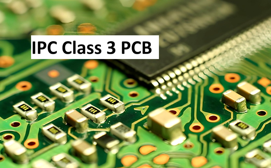
IPC Class 3 defines stringent acceptability requirements for electronic products where continued performance and reliable operation are critical. PCB requirements are specified across several IPC standards, including IPC-6012 for qualification and performance specifications for rigid printed boards, together with applicable design and acceptability standards.
Compared with Class 1 and Class 2, Class 3 products generally require tighter control of manufacturing processes, materials, workmanship, inspection, and reliability-related characteristics. Depending on the PCB construction and applicable specification, manufacturers may need to control factors such as plated-hole integrity, conductor geometry, dielectric spacing, solderability, cleanliness, and dimensional tolerances more carefully.
Class 3 requirements are particularly relevant to applications where PCB failure can result in significant system downtime, safety concerns, or loss of critical functionality. Examples can include aerospace and defense electronics, certain automotive safety systems, industrial control equipment, medical electronics, and other high-reliability applications.
It is important to note that IPC Class 3 is an acceptability classification, rather than a guarantee that a PCB will never fail. Product reliability also depends on the design, materials, operating environment, manufacturing process, assembly quality, testing, and qualification requirements of the specific application.
IPC PCB Classification System
IPC’s classification system provides different levels of acceptability according to the intended use of an electronic product.
Class 1: General Electronic Products
Class 1 applies to products where the primary requirement is the function of the completed assembly. These products are generally associated with consumer or general-purpose applications where limited product life or occasional imperfections may be acceptable.
Class 2: Dedicated Service Electronic Products
Class 2 applies to products where continued performance and extended service life are important, but uninterrupted operation is not necessarily essential. Telecommunications equipment, industrial electronics, and many commercial products may fall into this category.
Class 3: High-Reliability Electronic Products
Class 3 applies to products where continued performance or performance-on-demand is critical. The intended application typically requires a higher level of manufacturing control and inspection because defects that may be acceptable under lower classifications can become unacceptable under Class 3 requirements.
The specific acceptance criteria should always be determined from the applicable IPC standards, product documentation, customer requirements, and manufacturing specifications rather than assuming that every Class 3 PCB uses identical dimensional limits.
Key IPC Class 3 PCB Requirements
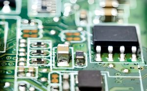
Compared with Class 1 and Class 2, Class 3 production requires greater attention to PCB design, fabrication, assembly, inspection, and process control.
The following are some of the most important considerations.
Plated Through-Hole Reliability
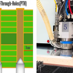
Plated through-holes (PTHs) are critical interconnection structures in multilayer PCBs. Their copper plating must maintain electrical continuity and mechanical integrity throughout manufacturing and the product’s intended operating conditions.
For Class 3 applications, plated-hole quality is particularly important because thermal cycling and mechanical stress can place significant strain on the plated copper barrel.
The required copper thickness and other acceptance criteria depend on the applicable IPC specification and board construction. Manufacturers must therefore verify the relevant IPC-6012 requirements rather than applying a single copper-thickness value to every PCB.
Proper control of drilling, desmear, electroless copper deposition, electrolytic copper plating, and thermal processing is essential for reliable plated-through-hole performance.
Annular Ring and Hole Registration
The annular ring is the copper area surrounding a drilled hole. Adequate annular ring is important because poor registration between the drill and copper pad can reduce mechanical and electrical reliability.
For Class 3 PCB Manufacturing, drill registration must be carefully controlled through:
- Accurate artwork registration
- Controlled lamination
- Precision drilling
- Appropriate pad dimensions
- Manufacturing compensation
- Automated optical and dimensional inspection where applicable
The exact minimum annular-ring requirements depend on the applicable IPC standard, PCB construction, and whether the feature is external or internal. Therefore, engineers should define the required values in the fabrication drawing instead of assuming a universal ±2 mil requirement.
Conductor Width and Spacing
Conductor width and spacing directly affect electrical performance, current-carrying capability, manufacturability, and insulation reliability.
The appropriate trace width depends on factors such as:
- Copper thickness
- Allowable temperature rise
- Current level
- Trace geometry
- PCB material
- Internal or external layer construction
- Manufacturing capability
Similarly, electrical spacing must be selected according to operating voltage, environmental conditions, insulation requirements, and the applicable design standard.
For this reason, the commonly quoted values below should be treated as example design targets rather than universal IPC Class 3 minimums:
| Copper Thickness | Example Trace Width | Approximate Current* | Example Spacing |
|---|---|---|---|
| 1 oz (35 µm) | ≥4 mil (100 µm) | Application-dependent | Application-dependent |
| 2 oz (70 µm) | ≥6 mil (150 µm) | Application-dependent | Application-dependent |
| 3 oz (105 µm) | ≥8 mil (200 µm) | Application-dependent | Application-dependent |
*Current capacity cannot be determined from copper thickness alone. Trace width, allowable temperature rise, layer position, thermal environment, and applicable design criteria must also be considered.
Solder Joint Quality
Solder joints provide both electrical and mechanical connections between components and the PCB. For high-reliability Class 3 assemblies, solder-joint quality must be carefully controlled because joints may experience repeated thermal cycling, vibration, mechanical stress, and environmental exposure.
Inspection should address characteristics such as:
- Proper solder wetting
- Adequate solder coverage
- Correct component alignment
- Solder bridges
- Voids where applicable
- Cracks
- Cold or disturbed solder joints
- Insufficient solder
- Excessive solder
The exact acceptance criteria vary according to the component type, package, soldering process, and applicable IPC assembly standard, such as IPC-A-610.
Through-hole solder fill should likewise be evaluated according to the applicable acceptance criteria rather than assuming that every Class 3 application universally requires 100% hole fill.
PCB Cleanliness Requirements
Cleanliness is an important factor in high-reliability PCB Manufacturing.
Contamination from flux residues, ionic materials, chemicals, dust, fingerprints, or other process residues can contribute to corrosion, leakage currents, electrochemical migration, and dendritic growth under suitable environmental conditions.
For Class 3 products, manufacturers should establish appropriate cleaning and contamination-control procedures based on the assembly process and end-use environment.
Common cleaning approaches may include:
- Aqueous cleaning
- Semi-aqueous cleaning
- Solvent-based cleaning where appropriate
- Vapor cleaning
- Ultrasonic cleaning for compatible assemblies
The correct cleaning method depends on component construction, materials, flux chemistry, PCB finish, and assembly process. Cleaning should also be validated rather than selected solely because a product is classified as Class 3.
Conformal Coating and Environmental Protection
Many high-reliability PCBs operate in environments involving humidity, chemicals, dust, temperature variation, vibration, or other environmental stresses.
A conformal coating can provide an additional protective barrier against moisture and contaminants. However, conformal coating is not automatically required for every IPC Class 3 PCB. Its use should be determined by the product’s environmental requirements and engineering specifications.
Common conformal coating materials include:
| Material | Key Characteristics | Typical Applications |
|---|---|---|
| Acrylic | Easy application and repair; good general-purpose moisture protection | Consumer and industrial electronics |
| Polyurethane | Good chemical and abrasion resistance | Automotive and industrial electronics |
| Silicone | Flexible and suitable for elevated-temperature environments | Aerospace and high-temperature electronics |
| Epoxy | Strong mechanical and chemical protection | Harsh-environment and specialized electronics |
Material selection should consider operating temperature, humidity, chemical exposure, repairability, flexibility, dielectric requirements, and long-term reliability.
IPC Class 3 PCB Design Rules Checklist
Engineers developing high-reliability PCBs should consider the following checklist during the PCB Design stage.
1. Plan the PCB Stackup Early
Define the layer stackup before detailed routing begins. Consider:
- Number of signal layers
- Power and ground planes
- Dielectric thickness
- Controlled impedance requirements
- Copper thickness
- Thermal requirements
- Material Tg and other material properties
- Manufacturability
For multilayer PCBs, the stackup should be developed together with the fabricator when tight tolerances or advanced structures are involved.
2. Optimize Pads and Vias
Provide adequate pad dimensions and annular rings for the selected manufacturing process. Where appropriate, teardrops can be used to improve the transition between pads and traces and increase resistance to certain manufacturing stresses.
Via dimensions should be selected according to the PCB fabrication process, aspect ratio, layer count, material system, and reliability requirements.
3. Control Trace Width and Spacing
Trace width should be calculated based on current requirements and allowable temperature rise rather than using a single fixed value.
Spacing should account for:
- Operating voltage
- Layer type
- Environmental conditions
- Insulation requirements
- Manufacturing capability
- Applicable IPC design rules
Engineers should also distinguish between general design recommendations and mandatory customer-specific requirements.
4. Optimize Power and Thermal Design
Use appropriate power and ground structures to reduce voltage drop and improve thermal performance.
Large copper areas and planes can be useful for:
- Current distribution
- Heat spreading
- Ground reference stability
- EMI control
- Power integrity
Copper balance across the PCB should also be considered during fabrication to reduce warpage and improve dimensional stability.
5. Plan Component Placement Carefully
High-power and high-speed components should be positioned according to thermal, signal-integrity, and electromagnetic requirements.
Polarity-sensitive components should use consistent orientation where possible. Adequate inspection, rework, and component-access space should also be considered during layout.
6. Follow Appropriate Pad Design Standards
Pad geometry should be matched to the selected component package and assembly process.
For BGA, QFN, fine-pitch ICs, and other advanced packages, engineers should carefully consider solder-mask openings, paste apertures, land patterns, and assembly tolerances.
IPC-7351 can be used as a reference for land-pattern design where applicable.
7. Clearly Define Manufacturing Requirements
When transferring a design to a PCB manufacturer, the fabrication documentation should clearly specify the required performance class and applicable standards.
A complete manufacturing package may include:
- Gerber or ODB++ data
- Drill files
- Stackup information
- Material requirements
- Copper thickness
- Surface finish
- Impedance requirements
- Hole sizes and tolerances
- Solder-mask requirements
- Controlled-impedance documentation
- Special inspection requirements
- IPC Class 3 requirements
Clearly defined documentation reduces ambiguity between the PCB designer, manufacturer, and assembly provider.
Advantages of IPC Class 3 PCB
An IPC Class 3 PCB is manufactured under stricter requirements than products intended for less demanding applications.
Potential benefits include:
Higher Manufacturing Control
More demanding inspection and process controls can help reduce defects that could affect long-term product performance.
Improved Interconnection Reliability
Careful control of plated holes, copper features, solder joints, and materials can improve the reliability of electrical and mechanical interconnections.
Better Suitability for Harsh Environments
When combined with appropriate materials, design practices, testing, and environmental protection, Class 3 manufacturing can support applications exposed to vibration, temperature cycling, humidity, and other demanding conditions.
Greater Process Traceability
High-reliability production often requires stronger documentation, inspection records, process controls, and manufacturing traceability.
Support for Critical Applications
These characteristics make Class 3 requirements relevant to applications where consistent performance and reliability are particularly important, including aerospace, defense, industrial, automotive, and medical electronics.
However, Class 3 classification alone does not automatically guarantee longer service life or lower signal loss. Those characteristics depend on the complete PCB design, material system, manufacturing process, assembly process, and operating environment.
Challenges of IPC Class 3 PCB Manufacturing
Although Class 3 production provides a rigorous framework for high-reliability PCB manufacturing, it also introduces additional challenges.
Higher Manufacturing Cost
Tighter process control, specialized equipment, additional inspection, higher-grade materials, and increased documentation can increase manufacturing costs.
More Complex Inspection
Manufacturers may need to perform more extensive inspection and verification, depending on the product requirements. These processes can include AOI, dimensional inspection, microsection analysis, electrical testing, X-ray inspection, and other qualification or acceptance procedures where applicable.
Tighter Process Control
Small deviations in drilling, registration, plating, solder mask, copper distribution, and lamination can become more significant when manufacturing high-reliability boards.
More Difficult Rework
Complex multilayer structures, fine-pitch components, BGAs, HDI structures, and high-density routing can make assembly and rework more challenging.
Greater Documentation Requirements
Class 3 projects often require detailed fabrication drawings, material specifications, inspection criteria, test requirements, and traceability records.
For these reasons, engineers should involve the PCB manufacturer early in the design process instead of waiting until the production stage.
IPC Class 3 PCB vs. Class 1 and Class 2
| Feature | IPC Class 1 | IPC Class 2 | IPC Class 3 |
|---|---|---|---|
| Primary focus | General functionality | Extended performance and service life | High reliability and continued performance |
| Typical application | Consumer/general electronics | Commercial and industrial electronics | High-reliability and critical applications |
| Manufacturing control | Standard | More controlled | More stringent |
| Inspection requirements | Application-dependent | More demanding | Generally more demanding |
| Defect tolerance | Higher for certain conditions | Lower | Lowest among the three classifications |
| Documentation | Standard | Detailed | Typically highly controlled |
| Cost | Generally lower | Moderate | Generally higher |
The table provides a general overview. The exact acceptance criteria must be determined from the applicable IPC standards and the customer’s product specification.
How to Manufacture an IPC Class 3 PCB
A reliable Class 3 production process should begin well before fabrication.
Step 1: Define the Application Requirements
Determine the operating environment, expected service life, electrical requirements, thermal conditions, mechanical stresses, and applicable regulatory or customer requirements.
Step 2: Develop the PCB Design
Create the schematic, stackup, layout, controlled-impedance structures, power distribution, thermal design, and component placement.
Step 3: Perform DFM and Reliability Reviews
Before production, conduct DFM analysis to identify potential manufacturing risks. For high-reliability applications, engineers should also review thermal cycling, mechanical stress, signal integrity, and other relevant reliability factors.
Step 4: Fabricate the PCB
The manufacturer controls drilling, plating, lamination, imaging, etching, solder-mask application, surface finishing, routing, and other fabrication processes according to the approved specifications.
Step 5: Perform Inspection and Testing
Depending on the design and customer requirements, inspection may include AOI, electrical testing, dimensional inspection, microsection analysis, X-ray inspection, impedance testing, and other verification procedures.
Step 6: Assemble and Inspect the PCB
During PCB Assembly, component placement, soldering, cleaning, inspection, and testing must be controlled according to the applicable assembly requirements.
Step 7: Verify Documentation and Traceability
Production records, material information, inspection results, test data, and other required documentation should be retained according to the project’s quality system and customer requirements.
Conclusion
IPC Class 3 PCB requirements are intended for electronic products where reliable performance is particularly important. Compared with lower IPC classifications, Class 3 production places greater emphasis on manufacturing control, interconnection integrity, inspection, documentation, and process consistency.
For engineers, achieving reliable Class 3 results starts with a well-planned PCB Design. Stackup selection, material choice, via and pad geometry, conductor width and spacing, thermal management, impedance control, and manufacturability should all be considered before fabrication begins.
For manufacturers, successful PCB Manufacturing requires precise process control, appropriate inspection, reliable equipment, qualified materials, and clear communication with the customer.
Kingda supports high-reliability PCB projects with professional PCB fabrication and assembly capabilities, helping engineers transform demanding designs into manufacturable and production-ready circuit boards.