How Long Does It Take to Learn PCB Design? PCB Design & PCB Manufacturing Guide
PCB Design is an essential skill for electronics hobbyists, students, and aspiring engineers. Whether you want to organize your personal electronics projects more effectively or eventually develop a product for mass production, designing circuits on a PCB is a natural step toward creating more reliable, compact, and professional electronic devices.
Learning PCB design can make your projects easier to build, test, troubleshoot, and manufacture. More importantly, it provides a foundation for exploring advanced areas such as high-speed electronics, RF circuits, multilayer boards, embedded systems, and HDI technology.
After understanding the benefits of learning PCB design, many beginners naturally ask:
How long does it take to learn PCB design?
There is no single answer. The learning time depends on your electronics background, familiarity with design software, project complexity, learning goals, and how consistently you practice.
For a beginner starting from zero, basic PCB design skills can often be developed within several weeks of regular study. Designing useful personal projects may take one to several months, while reaching a professional level can require years of practical experience.
This guide explains the major factors that affect the learning process and provides a practical roadmap for learning PCB Design and understanding how it connects to PCB Manufacturing.
Factors That Affect How Long It Takes to Learn PCB Design

Several factors determine how quickly you can become comfortable with PCB design.
1. Your Electronics Background
A solid understanding of basic electronics is one of the most important foundations for PCB design.
You should understand concepts such as:
- Voltage
- Current
- Resistance
- Capacitance
- Inductance
- Ohm’s law
- Power
- Series and parallel circuits
- Basic semiconductor concepts
- Digital and analog signals
PCB design is much more than drawing lines between components in software. A PCB layout must represent a circuit that works electrically and can be manufactured reliably.
If you have already built circuits on a breadboard, you may already understand some of these fundamentals. If you are starting completely from scratch, it is better to learn basic electronics before focusing heavily on PCB layout.
Useful learning resources include electronics textbooks, educational websites, laboratory projects, video tutorials, and introductory electronics courses.
With consistent study and hands-on practice, many beginners can develop a working understanding of basic circuits within a few weeks to a couple of months. The exact timeframe varies significantly between learners.
2. PCB Design Software Skills
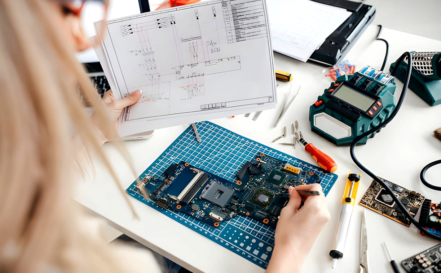
Another major factor is your familiarity with ECAD software.
Popular PCB design platforms include:
- KiCad
- EasyEDA
- Altium Designer
- Autodesk Fusion Electronics
- OrCAD
- Cadence Allegro
For beginners, KiCad and EasyEDA can provide accessible ways to learn fundamental schematic and PCB layout concepts. Professional engineers may eventually need more advanced commercial tools depending on their employer, industry, and project requirements.
When learning PCB design software, you should become familiar with:
- Schematic capture
- Component libraries
- PCB footprints
- Net management
- Board outlines
- Layer management
- Design rules
- Component placement
- PCB routing
- Copper pours
- Ground planes
- Design Rule Checking (DRC)
- Gerber generation
The software itself is usually not the hardest part. The more important challenge is understanding why components and traces should be arranged in a particular way.
A beginner may learn the basic interface within several days or a few weeks, but becoming comfortable with the complete workflow usually requires much more hands-on practice.
3. Consistent Practice
Consistency is arguably one of the most important factors in learning PCB design.
Even if you understand electronics theory and software operation, designing a real PCB introduces new challenges.
You need to learn how to:
- Interpret schematics
- Select appropriate footprints
- Place components logically
- Route traces efficiently
- Manage power distribution
- Create ground planes
- Control clearances
- Avoid signal interference
- Meet manufacturing constraints
- Check the design before fabrication
The fastest way to improve is to build real projects and learn from mistakes.
Instead of spending all your time watching tutorials, try to complete small PCB projects from schematic to manufactured board.
A Practical PCB Design Learning Roadmap
A structured learning path can make the process easier to manage.
Step 1: Learn to Read and Create Schematics
The first major skill is understanding circuit schematics.
You should be able to identify common components and understand how they interact electrically.
More importantly, learn how to convert a circuit you have built on a breadboard into a proper schematic.
At this stage, you should understand:
- Symbols
- Nets
- Power connections
- Ground connections
- Component values
- Signal paths
- Input and output connections
For many beginners, this stage can take several weeks of regular practice.
Step 2: Learn the PCB Design Software Workflow
Once you understand schematics, begin learning how to convert a schematic into a PCB layout.
A typical workflow includes:
Schematic → Footprint Assignment → PCB Layout → Component Placement → Routing → Design Rule Check → Manufacturing Files
Start with a simple two-layer board.
Practice:
- Creating board outlines
- Assigning footprints
- Placing components
- Routing traces
- Creating copper pours
- Adding mounting holes
- Setting design rules
- Running DRC
- Generating Gerber files
You should also learn how to create or modify custom footprints because not every component will necessarily be available in the default library.
With consistent practice, many learners can become comfortable designing simple PCBs within one to two months.
Step 3: Build Your First Simple PCB
Once you understand the basic workflow, design a small project.
Good beginner projects include:
- LED boards
- Sensor boards
- Simple power supply boards
- Button or switch boards
- Microcontroller breakout boards
- Simple Arduino-compatible circuits
A simple project teaches you something that tutorials cannot fully reproduce: the complete transition from a digital design to a physical circuit board.
Before manufacturing, check:
- Component footprints
- Trace clearances
- Board dimensions
- Mounting holes
- Polarity markings
- Connector orientation
- Copper pours
- DRC results
Then generate the required manufacturing files, such as Gerber files and drill data, and send them to a PCB manufacturer.
The turnaround time for a manufactured prototype depends on the manufacturer, board specifications, shipping method, and production service selected. Therefore, a fixed delivery period should not be treated as a universal expectation.
Step 4: Move to More Complex Designs
Once you are comfortable with simple two-layer boards, begin working on more sophisticated circuits.
Potential projects include:
- Operational amplifier circuits
- Microcontroller boards
- Sensor systems
- Motor controllers
- Power management circuits
- Arduino-based systems
- ESP32 projects
- STM32 development boards
These projects introduce additional concepts such as:
- Power distribution
- Decoupling capacitors
- Ground planes
- Analog and digital separation
- Return current paths
- Thermal management
- EMI and EMC considerations
At this point, you are no longer simply learning how to operate PCB software. You are learning how to make engineering decisions.
Step 5: Learn Multilayer PCB Design
After becoming comfortable with two-layer boards, you can move into multilayer PCB Design.
Multilayer PCBs provide additional routing layers and can include dedicated power and ground planes.
You may begin learning about:
- Four-layer PCB stackups
- Six-layer and eight-layer stackups
- Reference planes
- Controlled impedance
- Differential pairs
- Via structures
- Signal integrity
- Power integrity
- Crosstalk
- EMI control
Multilayer design requires a stronger understanding of electrical behavior because the physical arrangement of layers can significantly affect signal performance.
This is also where PCB Design becomes closely connected to PCB Manufacturing. Stackup selection, via structures, copper thickness, dielectric materials, minimum trace widths, and fabrication tolerances all need to be considered before production.
Step 6: Explore Advanced PCB Design
As your experience increases, you can move into specialized areas such as:
High-Speed PCB Design
High-speed designs require attention to:
- Impedance control
- Differential pairs
- Signal integrity
- Return paths
- Crosstalk
- Transmission lines
- Via discontinuities
- Timing
RF PCB Design
RF and microwave PCB design introduces additional considerations involving:
- Controlled impedance
- Transmission lines
- Grounding
- Component placement
- RF materials
- Electromagnetic coupling
- Signal loss
HDI PCB Design
High-Density Interconnect (HDI) PCB technology uses advanced structures such as:
- Microvias
- Blind vias
- Buried vias
- Fine-line routing
- Fine-pitch components
- Sequential lamination
HDI design requires close cooperation between the designer and PCB manufacturer because advanced fabrication capabilities directly affect achievable design rules.
How Long Does It Take to Learn PCB Design?
Instead of using one fixed number, it is more useful to divide PCB design learning into different levels.
| Skill Level | Typical Learning Focus | Approximate Time* |
|---|---|---|
| Beginner | Basic electronics and schematic reading | Several weeks |
| Basic PCB Design | Simple two-layer PCB layouts | 1–2 months |
| Intermediate | Microcontrollers, power, sensors, multilayer basics | Several months |
| Advanced | High-speed, RF, impedance, complex multilayer designs | 1–2+ years |
| Professional | Production-level engineering and specialized design | Several years of practical experience |
*These are general learning ranges rather than fixed requirements. Individual progress can vary considerably depending on prior knowledge, practice frequency, project complexity, and professional exposure.
The important point is that becoming able to design a simple PCB and becoming a professional PCB designer are two very different milestones.
You may be able to create your first functional PCB within a few weeks or months, but developing professional-level judgment requires experience with real products, manufacturing constraints, debugging, testing, revisions, and production feedback.
PCB Design Skills You Should Develop
If your goal is to become proficient rather than simply complete one PCB project, focus on several interconnected skills.
Electrical Engineering Fundamentals
Understand how circuits behave before worrying about sophisticated PCB layouts.
Schematic Design
Learn how to represent electrical connections clearly and logically.
Component and Footprint Selection
Understand electrical specifications as well as package dimensions, thermal requirements, and assembly constraints.
PCB Layout
Develop good habits for component placement, routing, grounding, power distribution, and signal management.
Design Rule Checking
Learn to identify clearance violations, unconnected nets, incorrect footprints, and other layout problems before manufacturing.
Manufacturing Awareness
Understand how your design will actually be fabricated and assembled.
This includes:
- Trace width
- Trace spacing
- Copper thickness
- Via dimensions
- Board thickness
- Surface finish
- Solder mask
- Silkscreen
- PCB stackup
- Panelization
- SMT assembly requirements
A designer who understands PCB Manufacturing can generally make more practical design decisions than someone who focuses only on software operation.
How to Learn PCB Design Faster
If you want to shorten the learning curve, focus on practical repetition rather than trying to learn everything at once.
Start Small
Do not begin with a complicated 12-layer high-speed board.
Start with a simple two-layer circuit and gradually increase complexity.
Build Real Projects
A completed PCB teaches you much more than an isolated tutorial.
Design → Manufacture → Assemble → Test → Troubleshoot → Revise.
This cycle is one of the most effective ways to develop practical skills.
Study Manufacturing Feedback
When a manufacturer identifies a DFM issue, do not simply change the design. Understand why the issue occurred.
This helps connect PCB layout decisions with actual manufacturing processes.
Learn from Failed Designs
A failed PCB is often an excellent learning opportunity.
Analyze:
- Why did the circuit fail?
- Was the schematic correct?
- Was the footprint correct?
- Was the component orientation correct?
- Was the trace routed correctly?
- Was the power distribution adequate?
- Was the ground return path appropriate?
- Was the PCB manufactured according to specification?
Gradually Increase Complexity
A useful progression is:
Simple LED Board → Sensor Board → Microcontroller Board → Power Board → Four-Layer PCB → High-Speed PCB → RF/HDI PCB
This approach allows you to develop new skills without becoming overwhelmed.
PCB Design Is a Continuous Learning Process
There is no final point at which you completely “finish” learning PCB design.
The industry continues to introduce:
- Faster interfaces
- Smaller components
- Higher layer counts
- Advanced PCB materials
- HDI technology
- Embedded components
- Advanced packaging
- Higher power densities
- New manufacturing processes
As a result, even experienced engineers continue learning.
The goal should therefore not be to memorize every PCB design rule. Instead, develop the ability to understand electrical requirements, evaluate manufacturing constraints, troubleshoot problems, and make informed engineering decisions.
Conclusion
So, how long does it take to learn PCB design?
If you are starting from zero, you may be able to understand basic electronics and create a simple PCB within several weeks to a few months with consistent practice. After several months, you can begin working on more complex microcontroller, power, and multilayer projects. Reaching a professional level in areas such as high-speed, RF, HDI, and production-oriented PCB design generally requires much more practical experience.
The exact timeline depends on your background, learning objectives, practice frequency, and the complexity of the projects you undertake.
The most effective approach is to learn progressively:
Learn Electronics → Read Schematics → Learn ECAD Software → Design a Simple PCB → Manufacture It → Test It → Troubleshoot It → Design More Complex PCBs
By following this process, you can gradually develop the skills required not only for PCB Design, but also for understanding PCB Manufacturing, PCB assembly, testing, and real-world product development.
Most importantly, do not wait until you think you know everything before building your first board. Start with a manageable project, learn from each revision, and gradually increase the complexity of your designs. Consistent hands-on practice is what ultimately turns PCB design knowledge into practical engineering skill.