How to Read a PCB Layout: PCB Design & PCB Manufacturing Guide
Printed circuit boards (PCBs) are essential components of modern electronic systems. Every PCB project has a specific design layout that contains critical technical information about the circuit, components, connections, and physical structure. Subsequent stages of development and manufacturing rely on this design data, which can also serve as a reference for future revisions, troubleshooting, maintenance, and product upgrades.
A PCB Layout is a technical visualization of an electronic circuit. It shows the physical locations of components, copper routing paths, connection points, and the interconnections between different functional sections of a circuit.
However, a PCB layout is much more than a flat graphical representation of a circuit. It contains important information about the board’s electrical functionality, mechanical structure, components, routing, layer configuration, and manufacturing requirements. An accurate layout is essential for achieving reliable PCB Design, manufacturability, electrical performance, and long-term durability.
For engineers, designers, technicians, and beginners, learning how to read a PCB layout is an important skill. This guide explains the key information contained in PCB layout files and provides a practical step-by-step approach to understanding them.
What Is a PCB Layout File?

A PCB Layout File is the design data created using PCB design software or an electronic design automation (EDA) tool. Depending on the software and development workflow, PCB projects may contain multiple file types and file extensions.
A schematic file primarily describes the logical relationships between components and electrical connections. By contrast, the PCB layout contains the physical implementation of those connections, including component placement, copper traces, vias, board outlines, layer assignments, footprints, and design rules.
Gerber files are different from native PCB layout files. Gerber data is primarily used to communicate manufacturing information for individual board layers, while drill files provide information about holes. Depending on the manufacturing package, additional files may contain solder mask, silkscreen, copper, paste, and other fabrication information.
The native PCB layout file generally contains much richer design information, including:
- Component footprints and placement
- Copper traces and routing
- Vias and pad structures
- Board outline and mechanical features
- Layer stackup information
- Net and connectivity information
- Design rules and constraints
- Copper pours and planes
- Component references and values
- Clearance and routing parameters
Manufacturers and PCB Assembly providers may use compatible CAD/EDA software, viewers, or manufacturing software to inspect this information. Therefore, understanding how to read a PCB layout is valuable for anyone involved in PCB Design, engineering, manufacturing, inspection, or troubleshooting.
Step-by-Step Guide to Reading a PCB Layout
Learning to read a PCB layout becomes much easier when the information is examined systematically. Beginners should start with the overall board structure before moving into individual components, layers, traces, and electrical connections.
A structured approach allows engineers to verify connectivity, confirm component placement, understand signal paths, and identify potential design or manufacturing issues before production.
1. Understand the PCB Design Files
The first step is to identify the correct version of the PCB Design files.
Check the file extensions, software version, revision number, and complete project package before opening the layout. A PCB project may contain schematic files, layout files, libraries, footprints, manufacturing outputs, drill files, and documentation.
It is important to confirm that the files are complete and that no components, libraries, or design information are missing. If a footprint or component appears incorrectly, determine whether the issue comes from the viewer, missing library data, or the original design.
For engineers analyzing an unfamiliar board, revision control is particularly important. Comparing an outdated layout with the current manufacturing files can lead to incorrect conclusions.
2. Use a Suitable PCB Layout Viewer
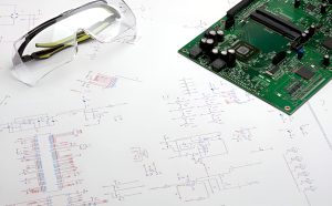
Use a compatible PCB layout tool or viewer to open the design.
Different EDA platforms may display PCB information differently. In some cases, an incompatible viewer may fail to display certain design objects, component models, layer information, or specialized features correctly.
Modern PCB viewers commonly provide both 2D and 3D visualization.
A 2D view is useful for examining:
- Copper traces
- Pads
- Vias
- Layer structures
- Board outlines
- Solder mask openings
- Silkscreen markings
- Component footprints
A 3D view provides additional information about component height, orientation, physical position, connectors, mechanical clearance, and enclosure compatibility.
For beginners learning how to read a PCB layout, switching between 2D and 3D views can make the relationship between electrical and mechanical design much easier to understand.
3. Identify the PCB Layers
Modern PCBs can contain multiple copper and dielectric layers, making layer identification one of the most important steps in layout analysis.
First determine the total layer count and identify the function of each layer. Depending on the board, these may include:
- Top copper layer
- Bottom copper layer
- Internal signal layers
- Power planes
- Ground planes
- Solder mask
- Silkscreen
- Paste layers
- Mechanical layers
For multilayer PCBs, it is important to understand the complete stackup rather than examining each copper layer independently.
For example, a high-speed PCB may use dedicated reference planes adjacent to signal layers to control impedance and reduce unwanted electromagnetic coupling. A power PCB may use large copper areas for current distribution and thermal management.
Understanding the stackup helps explain why a trace changes layers through a via and how signals or power are distributed throughout the board.
4. Identify Electronic Components
Electronic components are the functional building blocks of a PCB. Their combination determines the electrical behavior of the circuit.
When reading a layout, examine each component’s:
- Reference designator
- Footprint
- Package type
- Physical dimensions
- Orientation
- Pin or pad configuration
- Placement location
The silkscreen layer can help identify components through reference designators such as R1, C1, U1, D1, L1, and J1.
The Bill of Materials (BOM) should also be compared with the layout when available. This is especially useful for identifying small components, hidden components, alternate part numbers, and components whose markings are difficult to read.
For example, an IC may be identified as U1 in the layout, while its exact manufacturer part number and electrical specifications are listed in the BOM.
5. Understand PCB Symbols and Layout Elements
In addition to components, a PCB layout contains many other objects that represent electrical and mechanical functions.
Common layout elements include:
- Pads
- Vias
- Through-holes
- Blind vias
- Buried vias
- Copper traces
- Copper pours
- Connectors
- Test points
- Jumpers
- Mounting holes
- Fiducial markers
- Component outlines
- Keepout areas
- Net labels
Each element has a specific purpose.
For example, a via provides an electrical connection between PCB layers, while a mounting hole may provide only mechanical attachment. A thermal via transfers heat between layers, while a signal via carries an electrical connection between routing layers.
Custom footprints may also contain specialized pad arrangements or mechanical features, so engineers should not assume that every unusual shape represents a standard component.
6. Identify Power and Ground Networks
Power distribution is one of the most important aspects of PCB analysis.
Start by identifying the major power input points and determine how power is distributed throughout the board. Look for power connectors, regulators, power planes, large copper areas, decoupling capacitors, and ground connections.
Pay particular attention to:
- Power input and output paths
- Ground planes
- Power planes
- Voltage regulators
- Decoupling capacitors
- High-current traces
- Thermal vias
- Ground stitching vias
Following the power path can help explain how different functional blocks receive their operating voltage.
For multilayer boards, the power and ground networks may not be immediately visible in a standard 2D view. Layer isolation, net highlighting, and connectivity tools can make these networks much easier to follow.
Before PCB Manufacturing, designers should verify that power and ground connections are complete and that there are no unintended interruptions, excessive voltage-drop risks, or insufficient current-carrying structures.
7. Trace Identification and Signal Path Analysis
PCB traces carry power, control signals, clocks, and data between components.
When analyzing traces, determine where each important net starts and where it terminates. Follow the route from one component pin to another and identify any vias or layer changes along the way.
Important aspects to check include:
- Trace width
- Trace length
- Routing direction
- Clearance
- Layer transitions
- Via structures
- Net connectivity
- Differential-pair routing
- High-speed signal paths
- Power routing
For complex multilayer boards, manually following every trace can be difficult. PCB design software usually provides net highlighting, connectivity inspection, and interactive routing tools that allow engineers to trace an entire electrical network.
Special attention should be given to high-speed signals, clocks, differential pairs, and sensitive analog signals because their routing geometry can directly affect signal integrity.
Important Considerations When Reading a PCB Layout
PCB engineers generally use a systematic approach when reviewing a design. As circuits become denser and more complex, the following practices can make layout analysis more efficient.
Start With the Power Architecture
Starting with the power input and major power components provides a useful overview of the circuit’s functional structure.
Identify the power source, regulators, distribution networks, and major loads before examining individual signal paths.
Divide the PCB Into Functional Blocks
Instead of analyzing the entire board at once, divide it into functional sections.
Typical blocks may include:
- Power management
- Microcontroller or processor
- Memory
- Analog circuits
- Communication interfaces
- Sensor circuits
- RF sections
- Motor control
- User interfaces
Analyzing each functional block separately makes it easier to understand how the circuit operates.
Use Standard Reference Designs
Many PCB circuits are based on established application circuits or reference designs.
When reviewing an unfamiliar board, comparing its architecture with a relevant reference design can help explain the purpose of specific components, filtering networks, power stages, and signal paths.
However, engineers should always verify the actual design rather than assuming that it exactly matches a reference circuit.
Use Layer and Net Color Coding
Modern PCB software allows engineers to assign different display colors to layers, nets, or circuit groups.
Color coding can make it easier to distinguish:
- Top and bottom copper
- Internal signal layers
- Power networks
- Ground networks
- Critical signals
- Differential pairs
- Functional blocks
This is particularly helpful when analyzing dense multilayer PCB layouts.
Pay Attention to Designer Notes
PCB designers may leave useful notes, comments, labels, mechanical references, or design documentation within the project.
These details can explain special manufacturing requirements, component restrictions, test points, assembly instructions, or mechanical constraints.
Do not ignore these notes when reviewing a PCB layout.
Review the Board Layer by Layer
A complex PCB should be examined layer by layer rather than viewed as a single flat drawing.
Review the copper routing, planes, vias, solder mask, silkscreen, mechanical features, and other relevant layers separately. This approach can reveal connections and design features that are difficult to identify in a combined view.
Check Silkscreen and Footprints
Silkscreen markings can help identify components and their orientation, while footprints define the physical interface between components and the PCB.
Check for:
- Reference designators
- Pin-1 indicators
- Polarity markings
- Component outlines
- Pad sizes
- Courtyard or clearance information
- Connector orientation
Incorrect footprint selection can cause serious assembly or functional problems even when the schematic itself is correct.
Examine Thermal Management Structures
Thermal management is another important part of PCB layout analysis.
Look for:
- Large copper areas
- Thermal vias
- Heat sinks
- Thermal pads
- Copper planes
- High-power component placement
- Heat dissipation paths
High-power components should generally have an appropriate thermal path. Thermal vias may transfer heat from exposed pads or copper regions into internal or bottom layers, where additional copper or a heatsink can help dissipate it.
Thermal design should therefore be considered alongside electrical routing and mechanical constraints.
PCB Layout vs. PCB Manufacturing Data
It is important to distinguish between a native PCB layout and manufacturing output files.
A native layout file contains the design information needed to edit and analyze the board. Manufacturing files, such as Gerber and drill files, communicate the physical information required by the fabrication process.
| Item | Native PCB Layout | Manufacturing Files |
|---|---|---|
| Purpose | Design and engineering | PCB fabrication and assembly |
| Editability | High | Limited |
| Component placement | Usually included | May be provided separately |
| Nets | Usually available | Generally not represented as complete logical networks |
| Layer information | Complete design structure | Individual manufacturing layers |
| Design rules | Often included | Usually not fully represented |
| Drill information | Included in design | Typically provided as drill data |
| PCB fabrication | Source design | Direct manufacturing reference |
Understanding this difference is essential for engineers working across PCB Design and PCB Manufacturing.
Why Learning to Read PCB Layouts Matters
The ability to read a PCB layout is useful in many engineering and manufacturing activities.
It can help engineers:
- Verify component placement
- Trace electrical connections
- Diagnose PCB faults
- Review power distribution
- Check routing quality
- Understand multilayer structures
- Support PCB assembly
- Investigate manufacturing problems
- Perform design reviews
- Prepare product revisions
- Support maintenance and repair
For manufacturers such as Kingda, accurate interpretation of PCB design data also helps bridge the gap between engineering requirements and manufacturing execution.
A strong understanding of PCB layouts allows engineers to identify potential issues before they become expensive manufacturing or assembly problems.
Common Mistakes When Reading a PCB Layout
Beginners often make several common mistakes when analyzing PCB layouts.
Looking Only at the Top Layer
A multilayer PCB cannot be fully understood by examining only the top copper layer. Internal signal, power, and ground layers may contain critical connections.
Confusing a Footprint With a Component
A footprint describes the physical mounting pattern. It does not necessarily provide the complete electrical or commercial identity of the component.
Ignoring the Stackup
The stackup determines the physical relationship between copper layers and dielectric materials. It is particularly important for impedance-controlled and high-speed designs.
Assuming Visual Proximity Means Electrical Connection
Two pads or traces may appear physically close without being electrically connected. Always verify the actual net or connectivity information.
Ignoring Manufacturing Requirements
A layout may appear electrically correct but still contain manufacturing risks, such as insufficient spacing, unsuitable hole sizes, inadequate copper width, or problematic component clearances.
This is why PCB Design and PCB Manufacturing should be considered together rather than as completely separate processes.
Conclusion
A PCB layout is much more than a graphical representation of an electronic circuit. It contains detailed information about component placement, routing, layers, vias, power distribution, grounding, mechanical structures, and manufacturing requirements.
Learning how to read a PCB Layout starts with understanding the design files and viewer, followed by identifying the layer stackup, components, footprints, power and ground networks, traces, and signal paths. Engineers can then move toward more advanced analysis, such as impedance control, thermal management, high-speed routing, and manufacturability.
With regular practice, reading PCB layouts becomes similar to reading an engineering blueprint. Whether the goal is design verification, troubleshooting, assembly, maintenance, or PCB Manufacturing, the ability to interpret layout data accurately is an essential engineering skill.
As PCB technology continues to advance toward higher density, faster signals, smaller form factors, and increasingly complex multilayer structures, efficient layout analysis will become even more important. Modern PCB software, 3D visualization, automated design-rule checking, and AI-assisted engineering tools can further improve the efficiency of PCB design review and analysis.