How to Detect a Short Circuit on a PCB: PCB Design & PCB Manufacturing Guide
Printed circuit boards (PCBs) have become essential components for implementing the electrical functions and performance requirements of modern electronic products. As products integrate more intelligent features into smaller form factors, electronic circuits are becoming increasingly dense and complex.
To accommodate this trend, PCB technology has evolved from simple single- and double-sided boards into sophisticated multilayer structures capable of supporting high component density and complex interconnections. Modern integrated circuits, including very-large-scale integration (VLSI) and ultra-large-scale integration (ULSI) devices, allow millions or even billions of transistors to be integrated into compact electronic systems.
This increasing density creates significant challenges for PCB Design, PCB Manufacturing, assembly, inspection, and maintenance. Even a small PCB may contain a highly complex electrical system with numerous power, signal, and ground networks.
During design, manufacturing, assembly, or repair, various PCB defects can occur. Among them, a short circuit is one of the most important electrical faults because it can cause excessive current, unstable operation, component damage, overheating, and, in severe cases, permanent PCB damage.
Therefore, understanding how to detect a short circuit on a PCB is an essential skill for PCB engineers, technicians, manufacturers, and electronics repair professionals.
What Is a Short Circuit and What Causes It?
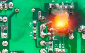
A short circuit on a PCB occurs when two electrical nodes that are not intended to be directly connected become electrically connected.
Under normal conditions, current and signals should follow the paths defined by the circuit design. An unintended conductive connection creates an alternative low-impedance path. Depending on where the short occurs, it can cause excessive current, voltage collapse, signal interference, overheating, or component failure.
Common causes of PCB short circuits include:
- PCB Design errors: Incorrect net assignments, insufficient clearance, overlapping traces, or incorrect layer connections can create unintended electrical connections.
- Solder bridges: Excess solder can connect adjacent pads, pins, or traces during PCB Assembly.
- Component misalignment: A misplaced component can cause its leads or terminals to contact nearby pads or copper features.
- Conductive contamination: Moisture, flux residues, dust, metal particles, or other contaminants can create unintended conductive paths under certain conditions.
- Multilayer PCB defects: Incorrect via connections, registration problems, or internal-layer defects can connect unintended networks.
- Repair and rework errors: Incorrectly installed jumper wires or repair traces can accidentally connect two different nets.
- Damaged insulation or solder mask: Mechanical damage can expose or bridge conductive areas that should remain electrically isolated.
- Copper fabrication defects: Manufacturing defects such as unwanted copper bridges or insufficient isolation can result in electrical shorts.
Understanding the possible failure mechanism is the first step toward determining how to detect PCB short circuits efficiently.
Symptoms of a PCB Short Circuit
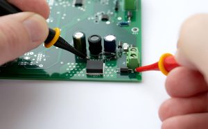
A PCB short circuit can produce several abnormal symptoms. However, these symptoms are not unique to shorts, so electrical testing should be used to confirm the diagnosis.
Common signs include:
- The product fails to power on.
- A power supply shuts down immediately after startup.
- A fuse repeatedly blows.
- The PCB draws excessive current.
- A voltage rail drops significantly below its expected value.
- Components or PCB areas become unusually hot.
- There is a burning smell or visible discoloration.
- The circuit repeatedly resets.
- The output signal becomes unstable or distorted.
- A power supply enters current-limiting or protection mode.
For example, if a low-voltage power rail is accidentally connected to ground, the power supply may enter current limiting rather than delivering its normal output. In other cases, the short may be localized and produce only a small temperature increase.
Therefore, identifying the exact short-circuit location requires a systematic PCB Testing process.
PCB Short Circuit Detection Techniques
Because modern PCBs use fine traces, small SMD packages, multiple layers, and high-density interconnects, the appropriate detection method depends on the board structure and the type of fault.
The following techniques range from simple visual inspection to advanced diagnostic equipment.
1. Visual Inspection
Visual inspection is usually the first step in PCB Troubleshooting because it is fast, inexpensive, and non-destructive.
Carefully examine the PCB under adequate lighting. A magnifying glass or microscope can be especially useful for boards containing fine-pitch components.
Look for:
- Solder bridges
- Excess solder
- Misaligned components
- Damaged pads
- Burn marks
- Carbonized areas
- Damaged solder mask
- Copper debris
- Foreign conductive particles
- Incorrect jumper wires
- Component leads touching adjacent conductors
Changing the viewing angle or using directional lighting can make solder bridges and surface contamination easier to see.
For high-density boards, optical inspection systems may be required because some defects are too small to identify reliably with the naked eye.
Visual inspection is useful but cannot detect many internal or electrically subtle short circuits. Therefore, it should normally be followed by electrical testing when a short is suspected.
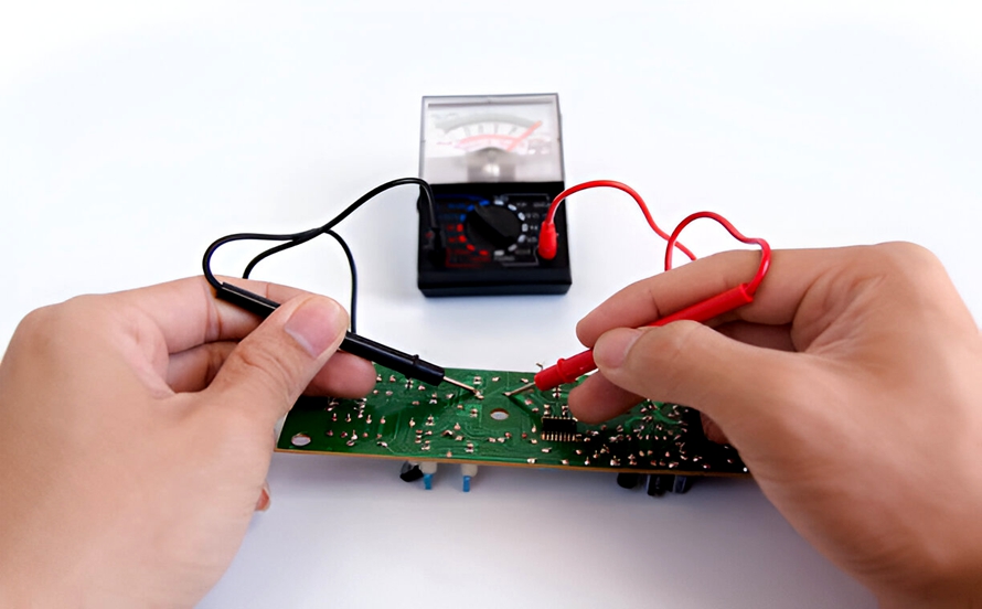
2. Manual Testing with a Multimeter
A digital multimeter is one of the most practical tools for detecting PCB shorts.
Before testing, disconnect the PCB from its power source and safely discharge relevant capacitors.
Set the multimeter to continuity mode or resistance mode.
Then:
- Identify the suspected power rail, signal node, or ground connection.
- Place one probe on the first node.
- Place the other probe on the second node.
- Observe the continuity indication or resistance reading.
- Compare the measurement with the expected circuit behavior.
A continuous beep may indicate a very low-resistance connection. However, a continuity beep does not automatically mean that a short circuit exists. Some PCB nodes are intentionally connected through low-resistance components, power planes, inductors, protection devices, semiconductor junctions, or other circuit paths.
Resistance mode can therefore provide additional information.
A very low resistance between a power rail and ground can be a strong indication of a short, but engineers should compare the reading with a known-good board or the circuit schematic whenever possible.
For complex boards, divide the circuit into functional sections and isolate the suspected power or signal network before taking further measurements.
3. Automated PCB Testing
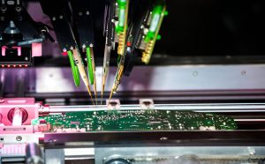
Manual inspection becomes increasingly inefficient as production volume and PCB complexity increase.
Automated inspection and electrical testing systems can provide much greater consistency.
Automated Optical Inspection (AOI)
AOI systems use cameras and image-processing algorithms to inspect PCB assemblies for visible manufacturing defects.
Depending on the system and inspection programming, AOI can identify problems such as:
- Solder bridges
- Component misalignment
- Missing components
- Incorrect component placement
- Soldering abnormalities
- Visible trace or pad defects
AOI is particularly useful for identifying surface-level causes of potential shorts during PCB assembly.
However, AOI primarily evaluates what the optical system can see. It cannot directly verify every internal electrical connection.
In-Circuit Test (ICT)
ICT uses a test fixture and electrical probes to access predefined test points or component nodes on the PCB.
The system can measure electrical characteristics such as:
- Continuity
- Resistance
- Voltage
- Component values
- Certain open and short conditions
ICT can be highly effective for production testing when the PCB has been designed with suitable test access.
However, ICT requires appropriate test-point planning, fixtures, programming, and test coverage. It is therefore more common in production environments than in hobbyist troubleshooting.
4. Advanced PCB Short Circuit Detection Methods
When visual inspection and basic multimeter testing cannot identify the fault, more advanced methods can be used.
Infrared Thermal Imaging
An infrared thermal camera can help locate a short circuit by identifying abnormal heat generation.
When a board is powered under a controlled and current-limited condition, a short may cause localized current flow and produce a hot spot.
Thermal imaging can help locate:
- Shorted power rails
- Overheating components
- Damaged ICs
- High-current leakage paths
- Localized copper heating
However, not every short generates enough heat to be visible. The method is most effective when the fault produces measurable thermal dissipation.
Current Injection and Thermal Localization
A controlled current can sometimes be injected into a suspected shorted power rail using a current-limited power supply.
The resulting voltage and thermal behavior can help engineers identify the fault location.
This method must be performed carefully. Excessive current can damage components and PCB traces, so the injected voltage and current should remain within safe diagnostic limits.
Magnetic or Current Tracing
Specialized current-tracing equipment can detect magnetic fields generated by current flowing through PCB conductors.
By scanning the board, engineers can sometimes identify where abnormal current is flowing and follow the path toward the shorted region.
This can be particularly useful when a short is difficult to locate visually.
Time-Domain Reflectometry (TDR)
TDR sends a controlled electrical signal through a transmission line and analyzes reflected signals caused by impedance discontinuities.
TDR is particularly useful for controlled-impedance traces, cables, backplanes, and other transmission-line structures.
A reflection at an unexpected location can indicate an impedance discontinuity, open circuit, short circuit, connector problem, or other defect.
However, TDR is not a universal PCB short-circuit detector. It is most useful when the suspected fault is associated with an appropriate transmission-line structure and the board/test setup supports meaningful TDR measurements.
5. Detecting Short Circuits in Multilayer PCBs
Finding shorts in a multilayer PCB can be significantly more difficult than finding them on a single-layer board.
Internal copper layers cannot be directly inspected from the surface, and blind vias, buried vias, microvias, and dense HDI structures can make electrical tracing more complicated.
Several methods can help.
X-Ray Inspection
X-ray inspection can reveal internal PCB and assembly structures that cannot be seen from the surface.
Depending on the system and board construction, X-ray can help identify:
- Hidden solder joints
- BGA connections
- Voids
- Internal structural abnormalities
- Component placement problems
- Some internal fabrication or assembly defects
X-ray is particularly valuable for assemblies containing BGA and other hidden solder joints.
However, X-ray imaging does not automatically identify every internal electrical short. Electrical testing may still be necessary to determine whether two internal nets are actually connected.
Cross-Section Analysis
Cross-sectioning physically cuts through the PCB so that internal layers, vias, plating, copper features, and dielectric structures can be examined under magnification.
This can provide highly detailed information about internal construction and manufacturing defects.
However, cross-section analysis is destructive, so it is generally reserved for failure analysis, process verification, or cases where non-destructive methods cannot provide sufficient information.
PCB Short Circuit Prevention During Design and Manufacturing
Prevention is generally more efficient than troubleshooting a completed board.
Short-circuit prevention should begin during PCB Design and continue through fabrication, assembly, inspection, and testing.
Use Adequate Trace Clearance
Maintain appropriate spacing between traces, pads, vias, and other conductive features.
The required clearance depends on voltage, manufacturing capability, environmental conditions, applicable standards, and the specific PCB fabrication process.
Run DRC and ERC
Before manufacturing, use the design software’s Design Rule Check (DRC) and Electrical Rule Check (ERC) functions.
These checks can help identify:
- Unconnected nets
- Incorrect clearances
- Routing conflicts
- Incorrect net assignments
- Certain design-rule violations
Automated checks cannot replace engineering review, but they can significantly reduce avoidable design errors.
Optimize Solder Mask Design
Appropriate solder-mask clearances and registration requirements can reduce the risk of unintended solder connections during assembly.
The solder-mask design should follow the PCB manufacturer’s fabrication capabilities.
Improve PCB Assembly Process Control
During PCB Assembly, accurate component placement and controlled soldering processes are essential.
Process controls such as solder-paste inspection, AOI, reflow-profile monitoring, and electrical testing can help identify defects before the product reaches final inspection.
Include Test Points
For production boards, appropriate test points can make PCB Testing much easier.
Test access should be considered during the initial design stage rather than added as an afterthought.
Perform Electrical Testing
A reliable production process may combine visual inspection, AOI, ICT, functional testing, and other inspection methods according to product requirements.
No single testing method can identify every possible PCB defect.
Common Mistakes When Detecting PCB Shorts
Several diagnostic mistakes can make short-circuit troubleshooting more difficult.
Assuming Every Continuity Beep Means a Short
Some circuits intentionally contain low-resistance paths. Always compare the measurement with the schematic and expected circuit topology.
Testing a Powered Board with the Wrong Mode
Resistance and continuity measurements should generally be performed on a properly powered-down circuit. Applying external voltage while using resistance or continuity mode can damage the meter or PCB.
Ignoring Capacitors
Large capacitors may initially appear as low resistance while charging from the multimeter’s test circuit. Allow the reading to stabilize and interpret it according to the circuit topology.
Focusing Only on Visible Areas
A multilayer PCB can contain defects that cannot be seen from the surface. Internal vias, planes, buried structures, and component connections may require electrical or imaging-based analysis.
Applying Excessive Current During Fault Localization
Current injection can be useful, but excessive current can turn a small fault into permanent PCB damage. Always use controlled and current-limited test conditions.
PCB Design and Manufacturing Considerations for Short-Circuit Prevention
Short-circuit prevention is closely related to both PCB Design and PCB Manufacturing.
During design, engineers should verify the schematic, netlist, stackup, trace spacing, via structure, component footprints, power distribution, and manufacturing rules.
During fabrication, controlled imaging, etching, drilling, plating, solder-mask application, and electrical testing help maintain the intended PCB structure.
During assembly, solder-paste printing, component placement, reflow, selective soldering, wave soldering, inspection, and functional testing all influence the probability of assembly-related shorts.
A professional manufacturer such as Kingda can support this process by integrating design-for-manufacturing considerations with PCB fabrication, assembly, inspection, and testing.
The goal is not simply to detect a short after it occurs, but to reduce the probability of creating one in the first place.
Conclusion
Knowing how to detect a short circuit on a PCB is an essential skill for PCB engineers, technicians, and electronics manufacturers.
A systematic approach should normally begin with visual inspection and then progress to multimeter measurements, electrical isolation, and more advanced techniques when necessary. AOI and ICT provide valuable support in production environments, while thermal imaging, controlled current injection, specialized current tracing, TDR, X-ray inspection, and cross-section analysis can help address more complex failures.
The most important point is that no single test method can detect every type of PCB short circuit. Surface shorts, power-rail shorts, multilayer defects, solder bridges, and transmission-line faults may require different diagnostic approaches.
At the same time, effective PCB Design and controlled PCB Manufacturing are essential for preventing shorts before they occur. Adequate spacing, reliable footprints, DRC/ERC verification, controlled assembly processes, test access, AOI, ICT, and functional testing can significantly improve PCB reliability.
For manufacturers and engineering teams, combining prevention, inspection, electrical testing, and systematic troubleshooting provides a more reliable path from PCB design to production.