How to Check if a PCB Is Working: PCB Design & PCB Manufacturing Guide
In the electronics industry, a printed circuit board (PCB) provides the electrical pathways and mechanical foundation needed to connect and power electronic components. From consumer electronics and industrial equipment to automotive systems and medical devices, PCBs are essential to the operation of modern electronic products.
But what should you do when an electronic device stops working?
Knowing how to check if a PCB is working is an important troubleshooting and maintenance skill. A systematic inspection can help determine whether the problem originates from the PCB itself, a component, the power supply, an interconnection, or another part of the system.
PCB testing can range from a simple visual inspection to detailed electrical measurements and advanced diagnostic techniques. By combining the appropriate methods, engineers can identify defects, verify PCB performance, and determine whether a board requires repair, rework, or replacement.
This guide explains how to check a PCB step by step, including visual inspection, multimeter testing, voltage measurements, oscilloscope analysis, AOI, thermal imaging, X-ray inspection, and functional testing.
What Is PCB Testing?
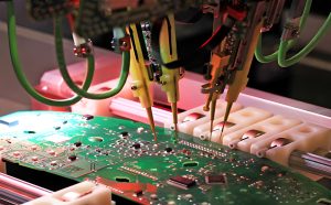
PCB testing is the process of inspecting and evaluating a printed circuit board to determine whether its physical structure, electrical connections, components, and functional behavior meet specified requirements.
Unlike testing a single electronic component, PCB Testing involves a network of interconnected components and conductive structures. A failure can originate from many sources, including:
- Open circuits
- Unintended short circuits
- Damaged components
- Incorrect component values
- Poor solder joints
- Component misalignment
- Damaged traces
- Defective vias
- Power-supply problems
- Signal-integrity issues
- Manufacturing defects
- Assembly defects
PCB testing is used at different stages of the product lifecycle. Manufacturers may test a PCB after fabrication and assembly, while engineers may test a board during prototype development, troubleshooting, repair, or maintenance.
The specific test method depends on the PCB’s complexity, application, production volume, and performance requirements.
How to Check if a PCB Is Working
There is no single measurement that can prove that every part of a PCB is functioning correctly. A board may have correct power rails but still contain a defective component or communication problem.
Therefore, how to check if a PCB is working should be approached systematically, starting with simple and low-risk inspections before moving to more advanced tests.
1. Perform a Visual Inspection
Before applying power, perform a thorough visual inspection. This is one of the simplest and most effective steps in PCB Troubleshooting.
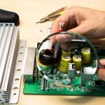
A magnifying glass or microscope may be useful for boards containing fine-pitch components, small passive devices, or high-density interconnects.
Check for Physical Damage
Look for:
- Cracks in the PCB
- Burn marks
- Delamination
- Broken connectors
- Scratches through copper traces
- Damaged solder mask
- Signs of overheating
Physical damage can interrupt electrical connections or cause intermittent failures.
Inspect Components
Look for components that are:
- Burned
- Cracked
- Swollen
- Discolored
- Loose
- Missing
- Installed incorrectly
For example, a swollen electrolytic capacitor may indicate excessive electrical or thermal stress, although visual symptoms alone cannot always identify the exact failure mechanism.
Inspect Solder Joints
Carefully inspect solder joints for:
- Solder bridges
- Insufficient solder
- Excessive solder
- Cracked joints
- Poor wetting
- Lifted pads
- Loose component leads
A defective solder joint can create either an open connection or an intermittent electrical connection.
Check PCB Cleanliness
Inspect the board for:
- Dust
- Flux residues
- Moisture
- Corrosion
- Conductive contamination
Contamination can contribute to leakage currents, corrosion, or electrochemical migration under certain environmental conditions.
Check Component Polarity and Orientation
Verify polarity-sensitive components such as:
- Diodes
- LEDs
- Electrolytic capacitors
- Certain ICs
- Some connectors and modules
Incorrect orientation can prevent a circuit from operating and may cause component damage when power is applied.
2. Perform Basic Electrical and Power Checks
After visual inspection, electrical measurements can provide more information about the PCB’s condition.
A digital multimeter (DMM) is one of the most useful tools for basic PCB Testing because it can measure resistance, continuity, DC voltage, and current, depending on the instrument.
However, the measurement method must be selected carefully to avoid damaging the PCB or producing misleading results.
Check Continuity
Set the multimeter to continuity mode and check appropriate circuit paths.
For example, engineers may verify:
- Ground connections
- Power paths
- Connector-to-trace connections
- Selected signal paths
- Fuses
- Jumpers
- Via connections
However, a continuity beep does not automatically mean that the PCB has a short circuit. A continuity tester simply indicates that the measured resistance is below its threshold. Many legitimate PCB connections are intentionally low resistance.
Therefore, continuity measurements should always be interpreted using the schematic, PCB layout, and expected resistance values.
Measure Resistance
Resistance measurements can help identify obvious shorts or abnormal connections when the board is unpowered.
For example, engineers may compare resistance between:
- Power and ground
- Adjacent signal nodes
- Different power rails
- Component terminals
A very low resistance between two nodes may indicate a problem, but some circuits naturally contain low-resistance paths. In-circuit measurements can also be affected by parallel components.
Measure DC Voltage
Once it is safe to power the board, measure important voltage points and compare the readings with the expected values.
Typical measurement points include:
- Main power input
- Voltage regulators
- IC supply pins
- Analog rails
- Digital power rails
- Reference voltages
- Ground
A significant difference between the measured and expected voltage may indicate a power-supply problem, excessive load, short circuit, defective component, or another circuit fault.
Check the Power Supply
Power-related faults are among the first issues to investigate when a PCB does not operate.
A controlled procedure may include:
- Verify the external power supply output.
- Confirm the PCB’s rated input voltage.
- Check resistance and potential shorts before powering the board when appropriate.
- Use a current-limited power supply if suitable.
- Apply power while monitoring current consumption.
- Measure critical power rails.
- Check components for abnormal heating.
A sudden current increase or collapse of a power rail can provide important clues about the fault location.
3. Use Advanced PCB Inspection and Testing
When visual inspection and basic electrical measurements cannot identify the problem, advanced testing methods can provide additional information.
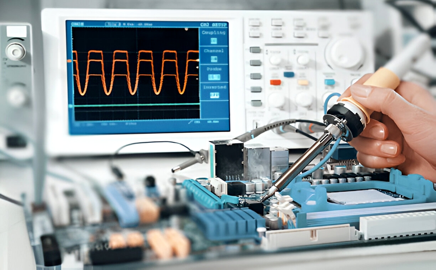
Oscilloscope Testing
An oscilloscope allows engineers to observe electrical waveforms directly.
It can be used to examine:
- Clock signals
- Reset signals
- PWM signals
- Analog waveforms
- Power-rail ripple
- Transient behavior
- Communication signals
For example, engineers can probe SPI, I²C, UART, CAN, or other interfaces and compare the observed waveform, timing, voltage levels, and signal integrity with the design requirements.
An oscilloscope is particularly useful when a PCB powers on but behaves incorrectly.
Logic Analyzer Testing
A logic analyzer is useful for digital systems where engineers need to observe logic states and communication protocols.
It can help analyze:
- SPI
- I²C
- UART
- GPIO activity
- Digital timing
- Protocol transactions
If a microcontroller appears to be running but communication fails, a logic analyzer can help determine whether the expected data is actually being transmitted.
Automated Optical Inspection (AOI)
Automated Optical Inspection (AOI) uses cameras and image-processing software to inspect assembled PCBs.
AOI can identify many visible assembly defects, including:
- Missing components
- Incorrect component placement
- Component polarity errors
- Solder bridges
- Solder-joint abnormalities
- Certain dimensional or placement deviations
AOI is widely used in PCB Assembly because it can inspect large numbers of boards consistently and quickly.
However, AOI is primarily a surface inspection method. It cannot directly verify every internal electrical connection or hidden solder joint.
Thermal Imaging
A thermal camera can help identify abnormal temperature distribution across a powered PCB.
Thermal inspection may reveal:
- Overheating ICs
- Shorted or overloaded components
- Abnormal power devices
- Hot connectors
- Unexpected current paths
- Uneven thermal distribution
For example, if one component becomes significantly hotter than comparable components, it may deserve further investigation.
Thermal imaging is especially useful for power electronics, motor controllers, power supplies, battery-management systems, and other high-current applications.
X-Ray Inspection
X-ray inspection provides a non-destructive way to examine certain structures that cannot be seen from the PCB surface.
It is particularly useful for assemblies containing:
- BGA packages
- QFN packages
- Hidden solder joints
- Internal structures
- Certain voids or soldering abnormalities
X-ray inspection can provide valuable information about hidden solder connections, but it should not be described as a universal method for detecting every PCB defect or internal electrical failure.
For certain complex investigations, additional techniques such as cross-section analysis may be required.
Functional Testing
Functional testing evaluates whether the complete PCB Assembly performs its intended function.
The board or finished electronic product is operated under defined conditions, and engineers verify expected inputs and outputs.
Functional testing may evaluate:
- Power-up behavior
- Sensor operation
- Communication
- Display functions
- Motor control
- Audio output
- Data processing
- Charging
- Protection circuits
- Analog and digital outputs
Functional testing is particularly useful because it evaluates the PCB under real or simulated operating conditions.
However, a board passing a functional test does not necessarily mean that every component or manufacturing feature is defect-free. Some latent or intermittent defects may require additional inspection.
PCB Testing Methods Comparison
| Testing Method | Main Purpose | Typical Defects or Problems |
|---|---|---|
| Visual Inspection | Physical examination | Damage, missing parts, solder defects |
| Continuity Test | Electrical path verification | Opens, selected connection problems |
| Resistance Test | Basic electrical diagnosis | Abnormal resistance, suspected shorts |
| Voltage Measurement | Power verification | Incorrect rails, regulator problems |
| Oscilloscope | Waveform analysis | Noise, timing, ripple, signal problems |
| Logic Analyzer | Digital communication | Protocol and timing issues |
| AOI | Automated visual inspection | Placement and solder defects |
| Thermal Imaging | Temperature analysis | Hot spots, overloads, abnormal heating |
| X-Ray | Hidden structure inspection | Hidden solder-joint issues, certain internal defects |
| Functional Test | System operation | Real-world operating failures |
The best approach is often to combine several methods rather than relying on a single test.
PCB Testing During PCB Design and Manufacturing
Effective testing begins before the physical PCB is manufactured.
During PCB Design, engineers should consider Design for Testability (DFT). This may include:
- Accessible test points
- Suitable probe clearances
- Programming interfaces
- Debug interfaces
- Clear component reference designators
- Accessible power rails
- Ground test points
- Appropriate connector access
Test points are especially important for production testing because they can provide automated equipment with reliable electrical access to critical nodes.
During PCB Manufacturing, manufacturers should also control fabrication and assembly parameters that affect test results.
Important manufacturing factors include:
- Layer alignment
- Trace width and spacing
- Via quality
- Copper thickness
- Plating
- Solder mask
- Surface finish
- Component placement
- Solder-paste printing
- Reflow soldering
- Cleaning where applicable
- Final inspection
A defect introduced during fabrication or assembly may later appear as an electrical or functional failure.
Common Mistakes When Checking a PCB
Knowing what not to do is just as important as knowing how to test a PCB.
Applying Power Without Inspection
Never assume an unknown PCB is safe to power immediately. A visual inspection and appropriate resistance checks can help identify obvious problems first.
Assuming Every Continuity Beep Indicates a Short
Continuity mode has a resistance threshold. It does not determine whether the connection is intentional.
Measuring Resistance on a Powered Circuit
Resistance measurements are normally performed on an unpowered circuit. Applying resistance-mode measurements to an energized circuit can produce incorrect readings or potentially damage the meter or circuit.
Using the Wrong Ground Reference
When measuring voltage or signals, use the correct circuit reference. An incorrect ground reference can produce misleading measurements.
Ignoring Component Datasheets
Expected voltages, current ranges, pin functions, and operating conditions should be verified against the relevant component documentation.
Touching the PCB Carelessly
Human contact can introduce ESD, contamination, or mechanical stress. Use appropriate ESD and handling procedures.
Relying on Only One Test
A PCB can pass one test and fail another. For example, a board may have correct DC power rails but still have a communication or timing problem.
Failing to Record Measurements
Recording actual measurements makes troubleshooting more systematic and allows engineers to compare a faulty board with a known-good board.
Best Practices for PCB Troubleshooting
A systematic troubleshooting process is generally more effective than randomly testing components.
A practical sequence is:
Visual Inspection → Resistance/Continuity → Power Verification → Voltage Measurements → Signal Analysis → Component Testing → Functional Testing
When possible, compare the faulty PCB with:
- The schematic
- PCB layout
- BOM
- Datasheets
- Expected measurement values
- A known-good PCB
This comparison can significantly narrow down the potential fault location.
For complex boards, divide the circuit into functional blocks such as:
Power Input → Protection → Regulation → Processing → Communication → Output
Testing each block independently can make fault isolation easier.
Conclusion
Understanding how to check if a PCB is working is an essential skill for electronics engineers, technicians, manufacturers, and maintenance personnel.
A reliable PCB Testing process should begin with a careful visual inspection and progress to continuity, resistance, voltage, and power measurements. When basic tests are insufficient, engineers can use oscilloscopes, logic analyzers, AOI, thermal imaging, X-ray inspection, and functional testing to investigate more complex problems.
Testing should also be considered during PCB Design and PCB Manufacturing, rather than being treated only as a final production step. Proper test-point placement, DFT considerations, controlled manufacturing processes, and clearly defined test criteria can make troubleshooting and production testing significantly more efficient.
Whether the goal is prototype validation, production quality control, field maintenance, or PCB repair, a systematic testing strategy helps identify faults more efficiently and supports consistent electronic product performance.
For manufacturers such as Kingda, integrating PCB fabrication, PCB Assembly, inspection, and testing into a controlled production process can provide a more consistent path from PCB Design to a reliable finished electronic product.