How to Test a PCB: PCB Design & PCB Manufacturing Guide
Printed circuit board (PCB) manufacturing and assembly follow a detailed and standardized process in which every step must be carefully controlled. Because errors can occur at virtually any stage of production, inspection and testing are essential before a board moves to the next process or is released to the customer.
For engineers and manufacturers, understanding how to test a PCB is critical for verifying electrical performance, identifying manufacturing defects, improving product reliability, and reducing the risk of field failures.
PCB testing can range from basic visual inspection and continuity checks to automated optical inspection (AOI), in-circuit testing (ICT), functional testing, environmental testing, and compliance testing. The appropriate method depends on the PCB design, assembly technology, application requirements, production volume, and reliability targets.
This guide explains the major PCB testing methods, preparation requirements, practical testing tips, common mistakes, and the relationship between PCB testing, PCB Design, PCB Manufacturing, and PCB Assembly.
Why Is PCB Testing Important?
PCBs are essential components in almost every modern electronic product. Whether used in consumer electronics, automotive systems, industrial equipment, telecommunications, medical devices, or power electronics, a PCB must deliver reliable electrical and mechanical performance.
Testing verifies whether the finished board meets its specified requirements. It can help identify:
- Open circuits and unintended short circuits
- Incorrect component placement
- Missing or damaged components
- Soldering defects
- Incorrect component values or orientations
- Manufacturing defects
- Power and signal integrity problems
- Functional failures
- Intermittent faults
- Environmental or long-term reliability problems
Effective PCB Testing also provides valuable feedback to engineering and manufacturing teams. When a recurring defect is discovered, engineers can determine whether the root cause is related to PCB Design, component selection, PCB Manufacturing, PCB Assembly, or test processes.
Early detection is particularly important in high-volume manufacturing because correcting a process problem early can prevent large numbers of defective boards from reaching later production stages.
PCB Testing Preparation
Before testing begins, the test process should be clearly defined. Engineers should understand the PCB’s schematic, layout, component specifications, electrical requirements, and acceptance criteria.
A practical preparation process includes the following steps.
Review the PCB Documentation
Prepare the necessary technical documentation, including:
- PCB schematic
- PCB layout
- Bill of materials (BOM)
- Gerber files and drill files when applicable
- Assembly drawings
- Component datasheets
- Test-point definitions
- Electrical specifications
- Functional test procedures
- Acceptance criteria
The documentation should clearly identify power rails, ground connections, signal paths, critical components, and expected measurement values.
Perform a Visual Inspection
Before applying power, inspect the PCB carefully. Look for:
- Missing components
- Incorrect component orientation
- Solder bridges
- Insufficient solder joints
- Lifted or damaged pads
- Burn marks
- Cracked components
- Damaged connectors
- Contamination or foreign materials
- Damaged solder mask
For high-density assemblies, magnification or automated inspection equipment may be necessary.
Prepare the Test Equipment
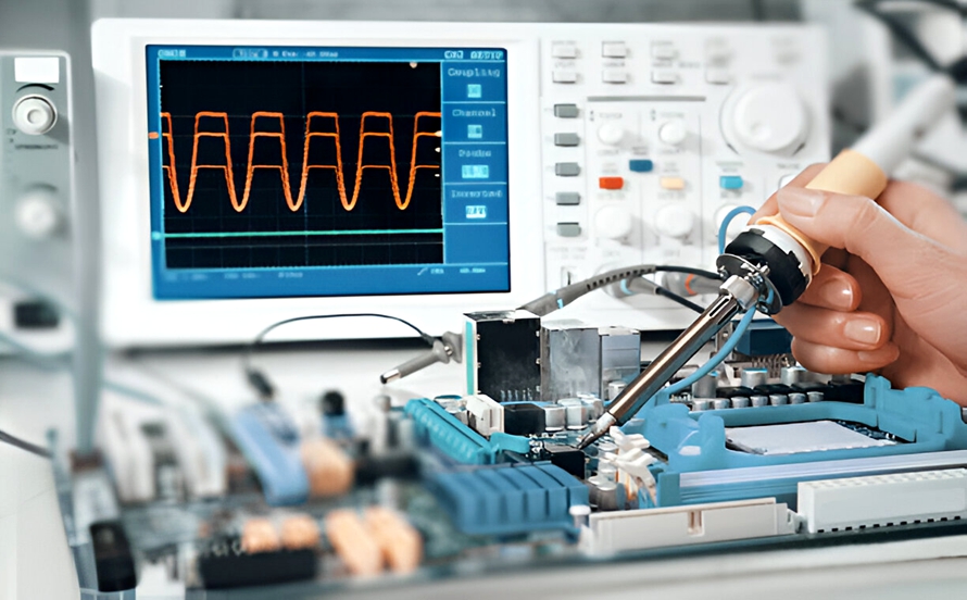
Depending on the test method, equipment may include:
- Digital multimeter
- Oscilloscope
- Logic analyzer
- LCR meter
- Programmable power supply
- Electronic load
- Function generator
- AOI system
- ICT fixture
- Functional test fixture
- X-ray inspection system
- Environmental test equipment
All measurement equipment should be appropriate for the expected voltage, current, frequency, and accuracy requirements.
Establish ESD Protection
Sensitive electronic components can be damaged by electrostatic discharge even when there is no immediately visible failure. Use an ESD-controlled workstation, suitable grounding, and appropriate handling procedures when required.
PCB Testing Methods
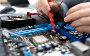
Different PCB testing methods detect different types of problems. No single test method can identify every possible defect.
The following methods are commonly used throughout PCB Manufacturing and PCB Assembly.
Layout Verification and Simulation
PCB testing begins before the physical board is manufactured.
During the PCB Design stage, engineers can use electronic design automation (EDA) software to verify schematic and layout information. Design Rule Checking (DRC) can identify issues such as:
- Insufficient clearance
- Incorrect trace widths
- Unrouted connections
- Inappropriate via sizes
- Manufacturing rule violations
- Component spacing problems
Electrical Rule Checking (ERC) may also be used at the schematic level to identify certain electrical design inconsistencies.
Simulation can further evaluate circuit behavior before fabrication. Depending on the design, engineers may simulate:
- Voltage and current behavior
- Transient response
- Frequency response
- Power integrity
- Signal integrity
- Thermal behavior
- Transmission-line characteristics
Simulation reduces design risk, but it cannot replace physical testing. Real PCBs can be affected by component tolerances, parasitic effects, manufacturing variation, assembly defects, temperature, contamination, and other factors that may not be fully represented in a simulation model.
Visual Inspection
Visual inspection is one of the simplest and most widely used PCB Testing methods.
It can be performed manually or with automated inspection equipment. Engineers inspect the board for physical defects such as:
- Missing components
- Wrong components
- Component misalignment
- Incorrect polarity
- Solder bridges
- Insufficient solder
- Excessive solder
- Cracked solder joints
- Damaged pads
- Contamination
- Mechanical damage
For complex PCB Assembly, Automated Optical Inspection (AOI) can rapidly inspect solder joints, component placement, polarity, and other visible characteristics.
However, AOI is primarily a surface inspection technique. It cannot directly verify every hidden solder joint or internal multilayer connection.
For BGA, QFN, and other packages with hidden solder joints, X-ray inspection can provide additional information about solder joints, voids, component placement, and certain internal structures.
Continuity Testing
Continuity testing verifies whether an intended electrical path is continuous.
A digital multimeter is commonly used for basic continuity checks. Depending on the circuit, engineers may check:
- Trace connections
- Connector pins
- Ground paths
- Power paths
- Jumpers
- Via connections
- Fuse paths
A continuity beep indicates that the meter detects a sufficiently low-resistance path according to its threshold. However, a beep does not automatically mean that a circuit is shorted.
For example, power and ground may intentionally be connected through low-resistance components or semiconductor structures under certain measurement conditions. Therefore, continuity measurements should always be interpreted using the schematic and expected circuit resistance.
For production environments, automated electrical testing can provide much more systematic coverage than manually probing individual points.
In-Circuit Testing (ICT)
In-Circuit Testing (ICT) uses a dedicated fixture and test probes to access specific points on a PCB Assembly.
ICT can be used to check characteristics such as:
- Component values
- Resistance
- Capacitance
- Inductance
- Diode characteristics
- Continuity
- Shorts
- Certain semiconductor connections
- Selected voltage or electrical conditions
ICT is particularly useful in volume manufacturing because the test process can be automated and repeated consistently.
However, ICT requires suitable test access and a properly designed fixture. Therefore, test points should be considered during PCB Design, especially for products that will be manufactured in significant quantities.
Functional Testing
Functional testing evaluates whether the assembled PCB performs its intended function.
During a functional test, the board is powered and provided with defined inputs. Test equipment then measures the resulting outputs and operating behavior.
Depending on the product, functional testing may evaluate:
- Supply voltages
- Communication interfaces
- Sensor inputs
- Digital outputs
- Analog signals
- Display operation
- Motor control
- RF performance
- Audio output
- Charging behavior
- Protection functions
For example, a controller PCB may need to receive sensor data, process the information, communicate through a digital interface, and activate an output. A functional test can verify this complete operating sequence.
Functional testing is highly valuable because it evaluates the assembled product under realistic operating conditions. However, it may not identify every underlying manufacturing defect, particularly when a defect does not affect the specific functional test being performed.
Burn-In Testing
Some electronic products are expected to operate continuously for long periods. A short electrical or functional test may confirm immediate performance but cannot fully demonstrate long-term stability.
Burn-in testing addresses this issue by operating the PCB under controlled conditions for a specified period.
During burn-in, engineers may monitor:
- Supply voltage
- Current consumption
- Temperature
- Output signals
- Communication status
- System stability
- Error conditions
The purpose is to identify failures that emerge during sustained operation or thermal/electrical stress.
Burn-in requirements should be defined according to the product’s application and reliability objectives rather than automatically applied to every PCB.
Environmental and Reliability Testing
For products exposed to demanding environments, environmental testing may be required in addition to standard electrical tests.
Depending on the application, testing can include:
- High-temperature testing
- Low-temperature testing
- Temperature cycling
- Humidity testing
- Thermal shock
- Vibration testing
- Mechanical shock
- Corrosion testing
- Moisture resistance testing
These tests can reveal weaknesses in materials, solder joints, connectors, PCB structures, and mechanical interfaces.
For example, an automotive PCB may experience substantial temperature variation and vibration, while an industrial PCB may need to withstand humidity, dust, chemical exposure, or continuous operation.
Environmental testing is therefore closely connected to material selection, stackup design, component selection, enclosure design, and PCB Manufacturing processes.
Compliance Testing
Electronic products may also need to satisfy regulatory and application-specific requirements.
Depending on the product and market, compliance testing may address:
- Electrical safety
- Electromagnetic compatibility (EMC)
- Electromagnetic interference (EMI)
- Environmental protection
- Ingress protection (IP)
- RoHS requirements
- Other applicable regulatory or industry standards
Compliance testing generally requires defined test configurations and procedures. Certain certifications or regulatory evaluations may be performed by qualified external laboratories or certification bodies.
These requirements should be considered during PCB Design, rather than being treated as an afterthought. For example, PCB layout, grounding, shielding, trace routing, filtering, creepage and clearance, and enclosure design can all affect EMC performance.
PCB Testing Tools
Different tools are suitable for different testing objectives.
| Testing Tool | Typical Application | Main Purpose |
|---|---|---|
| Digital Multimeter | Basic troubleshooting | Voltage, resistance, continuity |
| Oscilloscope | Signal analysis | Waveforms, noise, timing, ripple |
| Logic Analyzer | Digital circuits | Logic states and communication protocols |
| LCR Meter | Passive components | Capacitance, inductance, impedance |
| Programmable Power Supply | Power testing | Controlled voltage/current |
| Electronic Load | Power systems | Load and regulation testing |
| AOI | PCB Assembly | Visible assembly defects |
| ICT | Production testing | Electrical/component verification |
| X-Ray | Hidden joints | BGA/QFN and internal inspection |
| Functional Test Fixture | Product testing | Real operating behavior |
The appropriate test equipment depends on the PCB’s electrical characteristics and the purpose of the test.
Practical PCB Testing Tips
A well-designed test process should be repeatable, traceable, and safe. The following practices can improve PCB Testing efficiency and reliability.
1. Use Appropriate ESD Protection
Protect ESD-sensitive components by using appropriate grounding, ESD workstations, wrist straps, mats, and handling procedures where required.
2. Control the Power-Up Process
Do not immediately connect an unknown or repaired PCB to an unrestricted power source.
When appropriate, use a current-limited bench supply and verify the expected resistance and power-rail conditions before applying full power.
3. Define Pass/Fail Criteria
Each test should have a clearly defined acceptance range.
Instead of simply recording “pass” or “fail,” record the actual measured values when practical. This makes it easier to identify trends and process drift.
4. Use Clearly Defined Test Points
Test points should be considered during PCB layout. Important power rails, grounds, communication signals, and critical nodes may require accessible test points.
Good test-point planning can simplify ICT, functional testing, troubleshooting, and production diagnostics.
5. Maintain Test Records
Record important information such as:
- PCB serial number
- Revision
- Test date
- Operator or test station
- Test equipment
- Firmware version
- Measured values
- Pass/fail results
- Failure codes
- Repair or rework information
Traceability is particularly important for regulated, safety-critical, and high-reliability products.
6. Calibrate Test Equipment
Measurement accuracy depends on the condition and calibration status of the test equipment. Instruments and automated test systems should be maintained and verified according to their applicable procedures.
7. Follow Safe Discharge Procedures
After testing, safely discharge capacitors and other stored-energy circuits when required. Do not assume that a powered-off PCB is immediately safe to touch.
8. Separate Defect Diagnosis from Process Improvement
When a PCB fails, do not simply repair the individual board and move on. Determine the root cause.
For example, repeated solder bridges may indicate an assembly-process issue, while repeated clearance violations may indicate a PCB Design problem.
Common PCB Testing Mistakes to Avoid
Even a well-defined test process can produce unreliable results if basic precautions are ignored.
Testing Without Reviewing the Schematic
Measuring resistance or continuity without understanding the circuit can lead to incorrect conclusions. Always compare measurements with the intended circuit behavior.
Assuming a Continuity Beep Means a Short
A continuity tester only indicates a low-resistance path according to its threshold. It does not know whether that connection is intentional.
Applying Full Power Too Early
A PCB with an unknown fault can draw excessive current when powered. Controlled power-up procedures can reduce the risk of additional component damage.
Relying on Only One Test Method
Visual inspection, continuity testing, ICT, AOI, functional testing, and environmental testing provide different types of information. Combining appropriate methods provides better coverage.
Ignoring Test-Point Design
If a PCB has no accessible points for important signals or power rails, troubleshooting and automated testing can become unnecessarily difficult.
Skipping Documentation
A test without clear procedures and acceptance criteria can produce inconsistent results between operators and production lines.
Treating Simulation as a Replacement for Physical Testing
Simulation is valuable during PCB Design, but it cannot reproduce every manufacturing, assembly, environmental, and component-related variation.
PCB Testing and PCB Design
Testing should influence the PCB design process from the beginning.
A test-friendly PCB design may include:
- Accessible test points
- Appropriate probe clearances
- Programming/debug interfaces
- Clear reference designators
- Adequate component spacing
- Suitable grounding
- Proper power distribution
- DFM considerations
- DFT considerations
- Clear polarity markings
Design for Testability (DFT) allows engineers to consider how the finished PCB will be inspected and tested before manufacturing begins.
For high-volume products, DFT can significantly affect fixture design, test coverage, production cycle time, troubleshooting efficiency, and manufacturing cost.
PCB Testing and PCB Manufacturing
PCB Manufacturing quality directly influences test results.
A reliable manufacturing process should control:
- Material quality
- Layer alignment
- Trace width and spacing
- Hole dimensions
- Plating
- Copper thickness
- Solder mask
- Surface finish
- Board cleanliness
- Electrical testing
- Final inspection
For assembled boards, additional controls are required for component placement, solder paste printing, reflow profiles, THT soldering, cleaning when applicable, and inspection.
A qualified PCB manufacturer such as Kingda can integrate manufacturing controls with inspection and testing requirements to improve consistency from prototype through production.
How to Choose the Right PCB Testing Method
There is no universal PCB testing method for every product. Engineers should select testing methods according to several factors:
- PCB complexity — simple single-sided boards may require less testing than HDI or high-layer-count boards.
- Production volume — automated testing becomes increasingly valuable at higher volumes.
- Product reliability requirements — automotive, medical, aerospace, and industrial products may require more extensive validation.
- Assembly technology — BGA, QFN, fine-pitch SMT, and mixed-technology assemblies may require specialized inspection.
- Electrical complexity — high-speed, RF, power, and mixed-signal boards require different measurement approaches.
- Test coverage — determine which defects each test method can actually detect.
- Cost and cycle time — balance test coverage with production requirements.
- Traceability requirements — determine what test data must be stored for each board.
A practical production strategy may combine visual inspection, AOI, electrical testing, functional testing, and targeted X-ray or environmental testing depending on the application.
Conclusion
PCB testing is not simply a final inspection step. It is an integral part of the complete PCB Design, PCB Manufacturing, and PCB Assembly lifecycle.
From design-rule verification and simulation to visual inspection, continuity testing, ICT, functional testing, burn-in, environmental testing, and compliance evaluation, each method addresses different aspects of PCB quality and reliability.
The most effective approach is to establish testing requirements early, design accessible test points, define clear acceptance criteria, use properly maintained equipment, document results, and investigate the root cause of failures.
For engineers and manufacturers learning how to test a PCB, understanding the strengths and limitations of each method is essential. A systematic testing strategy can help reduce defects, shorten troubleshooting time, control manufacturing costs, improve product reliability, and reduce the risk of failures after shipment.
With appropriate PCB Design, controlled PCB Manufacturing, professional PCB Assembly, and well-planned testing, manufacturers such as Kingda can help customers achieve consistent PCB quality from prototype development through mass production.