How to Repair Broken PCB Traces: PCB Design, PCB Manufacturing & Repair Guide
Electronic technology is evolving rapidly, with manufacturers competing to develop products that are smaller, more powerful, more functional, and more cost-effective. At the heart of these electronic products are dense electrical circuits mounted on dielectric substrates known as printed circuit boards (PCBs).
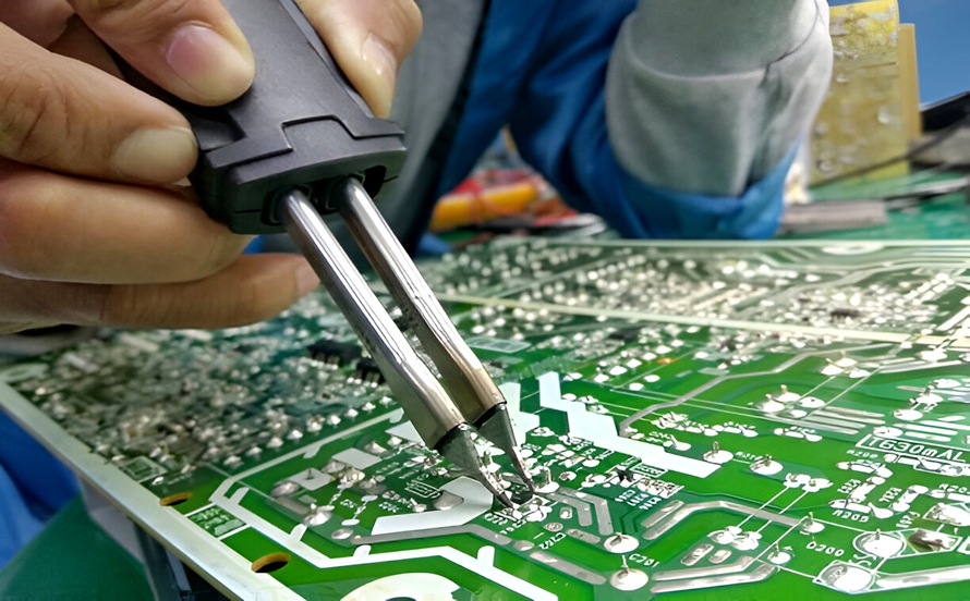
As circuit density continues to increase, the possibility of PCB failures also increases. These failures can result from manufacturing defects, design problems, component damage, improper handling, mechanical stress, overheating, or environmental exposure. One common problem is a damaged or broken PCB trace, which can directly affect the electrical performance and reliability of the entire device.
Learning how to repair broken PCB traces is therefore an important skill for electronics engineers, technicians, and repair professionals. A properly repaired trace can restore electrical continuity and extend the service life of an otherwise functional PCB.
This guide explains what PCB traces are, how to diagnose broken traces, which tools are required, and how to repair damaged PCB traces using practical repair techniques.
What Is a PCB Trace?
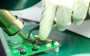
A PCB trace is a conductive pathway that electrically connects components, pads, vias, and other circuit elements on a printed circuit board.
Copper is the most commonly used trace material because it offers excellent electrical conductivity, good thermal conductivity, relatively low cost, and good compatibility with PCB manufacturing processes.
Important PCB trace design parameters include:
- Trace width
- Trace length
- Copper thickness
- Clearance
- Current-carrying capacity
- Impedance
These parameters must be carefully considered during PCB Design because they directly influence electrical performance, thermal behavior, signal integrity, and electromagnetic interference (EMI).
A damaged trace can interrupt the intended electrical connection. Depending on the circuit, even a very small break can cause an open circuit and prevent the entire electronic system from functioning correctly.
How to Diagnose a Broken PCB Trace
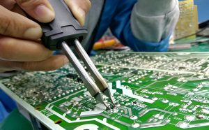
Modern PCB designs often contain narrow traces, small component pitches, and densely packed routing. As a result, identifying a damaged trace can sometimes be difficult.
Before attempting PCB Repair, the damaged area should be accurately identified.
Perform a Visual Inspection
Start with a careful visual inspection under good lighting.
Look for visible abnormalities such as:
- Scratched or broken copper
- Burn marks
- Discoloration
- Lifted pads
- Cracked solder joints
- Corrosion
- Physical damage
- Signs of overheating
A magnifying glass can help identify small defects. For fine-pitch or high-density boards, a microscope may be required.
Visual inspection is often the first and simplest step in determining how to repair broken PCB traces.
Perform a Basic Electrical Test
A multimeter can be used to check the continuity of a suspected PCB trace.
Set the multimeter to an appropriate continuity or resistance mode and place the probes at two points that should be electrically connected.
A continuous trace should normally show continuity or a low resistance value, depending on the circuit. A broken trace may show an open circuit or an unexpectedly high resistance.
When diagnosing a complex board, always consider the surrounding circuit because other components or parallel paths can affect the measured resistance.
Use Advanced Inspection and Testing Methods
For complex or high-density PCBs, advanced inspection techniques may be necessary.
AOI
Automated Optical Inspection (AOI) uses high-resolution imaging systems to inspect PCB surfaces for defects such as missing copper features, trace discontinuities, solder defects, and other manufacturing problems.
AOI is particularly useful in production environments because it can inspect large numbers of PCBs consistently.
X-Ray Inspection
Some PCB defects cannot be identified through visual inspection because they are located beneath components or inside multilayer structures.
X-ray inspection can reveal hidden defects such as internal connection problems, solder-joint issues, and certain defects within multilayer PCBs.
Time-Domain Reflectometry
Time-Domain Reflectometry (TDR) is an electrical measurement technique that sends a fast electrical signal through a conductive path and analyzes reflected signals.
For suitable transmission-line structures, TDR can help identify impedance discontinuities and estimate the location of a fault along the interconnect.
Because TDR requires specialized equipment and appropriate signal structures, it is generally more applicable to advanced PCB troubleshooting than simple low-speed trace repair.
What Tools and Materials Are Needed for PCB Trace Repair?
Having the correct tools is essential when repairing damaged PCB traces.
Depending on the severity and location of the damage, a basic PCB repair workstation may include:
Soldering Iron
A temperature-controlled soldering iron is used to heat solder and create electrical connections between the PCB trace, repair wire, and copper pads.
Temperature control is particularly important because excessive heat can damage the PCB substrate, solder mask, copper pads, and nearby components.
Multimeter
A multimeter is used to verify electrical continuity before and after the repair.
Testing before repair helps confirm the location of the open circuit, while testing after repair verifies that the new connection has restored electrical continuity.
Magnifier or Microscope
A magnifying glass or microscope allows technicians to inspect fine traces, solder joints, pads, and damaged areas.
For modern high-density PCBs, optical magnification is often necessary because the damaged trace may be too small to inspect accurately with the naked eye.
Scraping or Cutting Tools
A fiberglass pen, precision scraper, or other suitable PCB repair tool can be used to carefully remove solder mask and expose intact copper near the damaged area.
Only a small amount of solder mask should be removed. Excessive scraping can further damage the copper trace or the surrounding PCB material.
Jumper Wire
A jumper wire can bridge a broken PCB trace and restore electrical continuity.
The repair wire should have an appropriate diameter and insulation for the circuit. For high-current applications, the wire must be capable of carrying the required current without excessive heating.
How to Repair a Broken PCB Trace
There are several ways to repair damaged PCB traces. The appropriate technique depends on the location and severity of the damage, trace width, current requirements, PCB structure, and accessibility.
Two common approaches are jumper-wire repair and conductive trace reconstruction.
1. Repairing a Broken Trace with a Jumper Wire
Jumper-wire repair is one of the most practical methods for restoring a broken PCB trace.
Follow these general steps:
- Confirm the damaged trace. Use visual inspection and a multimeter to verify that the trace is electrically open.
- Expose intact copper. Carefully remove a small section of solder mask from both sides of the damaged area using a suitable precision tool.
- Clean the exposed copper. Remove contamination or oxidation so that the repair solder can bond properly.
- Apply a small amount of flux. Flux can improve solder wetting and help establish a reliable connection.
- Prepare the jumper wire. Cut an appropriate length of insulated wire and strip a small amount of insulation from both ends.
- Tin the wire ends. Apply a small amount of solder to the exposed wire.
- Solder one end of the jumper wire. Attach it to the exposed copper on one side of the damaged trace.
- Solder the other end. Connect the other end to the intact trace or appropriate pad on the opposite side of the break.
- Secure the repair. Use an appropriate insulating coating, epoxy, or PCB repair material to mechanically secure the wire when necessary.
- Test the repaired trace. Use a multimeter to confirm electrical continuity.
The jumper wire should follow a safe routing path and must not create accidental contact with adjacent traces, pads, or conductive surfaces.
2. Reconstructing or Reinforcing the Damaged Trace
For certain PCB repairs, the damaged copper can be reconstructed or reinforced rather than simply bypassed with a wire.
A typical repair process may include:
- Clean the damaged area using an appropriate PCB-safe cleaning method.
- Carefully remove damaged or loose copper.
- Expose a small amount of intact copper on both sides of the damaged section.
- Clean the exposed copper and apply flux.
- Position an appropriate copper repair material or replacement conductor across the damaged section.
- Solder the repair material to the intact copper.
- Check that the repaired conductor is properly aligned and mechanically stable.
- Apply an appropriate insulating or protective material after the solder joint has been inspected.
- Allow the repair material to cure if required.
- Perform electrical continuity testing.
For traces carrying significant current or signals requiring controlled impedance, the replacement conductor must be appropriately sized and routed. A simple wire repair may not reproduce the original electrical characteristics of a high-speed or impedance-controlled trace.
Guidelines for PCB Trace Repair
PCB trace repair should be performed carefully because an incorrect repair can create additional failures.
Match the Required Current Capacity
The replacement conductor should be capable of carrying the same or greater current than the original trace under the intended operating conditions.
For high-current traces, simply using a very thin jumper wire can introduce excessive resistance and heating.
Control the Soldering Temperature
Excessive heat can damage:
- Copper traces
- Solder pads
- Solder mask
- PCB laminate
- Nearby components
- Plated-through holes
Use an appropriate soldering temperature and minimize the amount of time the soldering iron remains in contact with the PCB.
Avoid Damaging Adjacent Traces
Modern PCBs can contain extremely narrow spacing between conductive features.
When removing solder mask or applying solder, take care not to scratch neighboring traces or accidentally create solder bridges.
A microscope is recommended when repairing fine-pitch or high-density PCBs.
Secure the Repair Mechanically
A repaired wire should not be left unsupported if the PCB will experience vibration, movement, or repeated mechanical stress.
Appropriate insulating or bonding materials can be used to secure the repaired conductor after electrical testing.
Test the PCB After Repair
A repair should never be considered complete simply because the new wire or conductor is physically attached.
Use a multimeter to confirm continuity and, where appropriate, perform additional electrical and functional tests.
For complex electronic assemblies, the repaired board may require complete functional testing before returning to service.
PCB Trace Repair vs. PCB Replacement
Repairing a damaged PCB trace can often be more economical than replacing an entire circuit board, especially when the damage is localized and the remaining PCB is in good condition.
However, repair is not always the best solution.
A replacement PCB may be more appropriate when:
- Extensive areas of the board are damaged
- Multiple internal layers are affected
- The PCB substrate is severely burned or delaminated
- Critical impedance-controlled structures are damaged
- High-reliability requirements cannot be verified after repair
- The repair cost approaches the cost of a new PCB
For professional applications, engineers should evaluate the electrical, mechanical, thermal, and reliability requirements before deciding whether to repair or replace the board.
Conclusion
Learning how to repair broken PCB traces is an important skill for electronics troubleshooting, PCB repair, and product maintenance. A broken trace can interrupt electrical continuity and cause an otherwise functional electronic system to fail.
The repair process generally begins with accurate diagnosis through visual inspection and continuity testing. Depending on the application, advanced methods such as AOI, X-ray inspection, or TDR may also be used to locate difficult-to-detect faults.
For localized damage, a properly sized jumper wire or reconstructed copper path can restore the connection. However, the repair must maintain adequate current capacity, electrical performance, mechanical stability, and insulation.
As PCB Design becomes increasingly dense and sophisticated, trace repair requires greater precision and attention to detail. Whether a board is being repaired, reworked, or evaluated during PCB Manufacturing, proper inspection and repair practices can extend its service life and reduce unnecessary replacement and electronic waste.
Kingda supports professional PCB Manufacturing, assembly, testing, and engineering requirements, helping customers move from PCB design concepts to reliable manufactured circuit boards.