How to Repair Broken PCB Traces: PCB Design, PCB Manufacturing & Repair Guide
As electronic technology continues to evolve, manufacturers are constantly developing devices that are smaller, more powerful, more affordable, and more feature-rich. Inside these products are increasingly dense electronic circuits mounted on dielectric substrates known as printed circuit boards (PCBs).
As circuit density increases, the possibility of failures also increases. These failures may result from PCB Manufacturing defects, PCB Design problems, improper handling, mechanical stress, overheating, or long-term use. One common issue is a damaged or broken PCB trace, which can directly affect the functionality and reliability of an electronic device.
Understanding PCB Trace Repair is therefore an important part of PCB maintenance and rework. In this guide, we will explain what PCB traces are, how to diagnose broken traces, which tools are required, and how to repair damaged traces using practical methods.
What Is a PCB Trace?
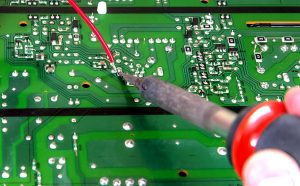
A PCB Trace is a conductive pathway that electrically connects components, pads, vias, and other circuit elements on a printed circuit board. Copper is the most common trace material because it offers excellent electrical conductivity, good thermal conductivity, wide availability, and relatively low cost.
Several parameters are particularly important when designing PCB traces, including:
- Trace width
- Trace length
- Copper thickness
- Trace spacing
- Current-carrying capacity
- Impedance requirements
These parameters must be carefully considered during PCB Design. For example, a trace that is too narrow for the required current may experience excessive heating, while inadequate spacing can increase the risk of short circuits and electrical interference.
For high-speed circuits, trace geometry also affects signal integrity, impedance, crosstalk, and electromagnetic interference (EMI). Therefore, repairing a damaged trace is not simply a matter of reconnecting two points—the replacement connection should also satisfy the electrical and mechanical requirements of the original design.
How to Diagnose a Broken PCB Trace
As PCB designs become more sophisticated, component pitches become smaller and traces become narrower. This makes PCB Troubleshooting and trace repair increasingly challenging.
Before attempting PCB Repair, the exact location and extent of the damage should be identified.
1. Perform a Visual Inspection
Start with a careful visual inspection under adequate lighting. Look for obvious signs of damage, including:
- Scratched or broken copper traces
- Burn marks
- Discoloration
- Cracked solder joints
- Lifted pads
- Mechanical damage
- Corrosion or oxidation
A magnifying glass can help identify minor damage. For fine-pitch or high-density boards, a microscope may be necessary to inspect narrow traces and small solder pads.
Visual inspection is often the first step in effective PCB Troubleshooting because it allows technicians to locate visible physical damage before performing electrical tests.
2. Perform a Continuity Test
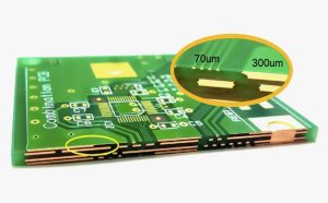
A multimeter can be used to determine whether a suspected trace is electrically continuous.
Set the multimeter to continuity mode or an appropriate resistance range, then place the probes at two points that should be electrically connected.
A normal connection should show continuity or a very low resistance. A broken trace may show no continuity or an abnormally high resistance.
However, the measured value must be interpreted according to the circuit. Some traces connect to components, parallel paths, or other circuitry, so a continuity reading does not always prove that the trace itself is intact.
3. Use Advanced Inspection and Testing Methods
For complex boards, advanced PCB Testing techniques may be required.
Automated Optical Inspection (AOI): AOI systems capture and analyze high-resolution images to identify visible defects such as trace damage, opens, insufficient solder, and other manufacturing defects.
X-Ray Inspection: X-ray inspection can reveal hidden defects that cannot be observed from the board surface, including certain internal-layer defects, voids, solder-joint problems, and structural issues.
Time-Domain Reflectometry (TDR): TDR sends a high-speed electrical signal through an appropriate transmission-line structure and analyzes reflected signals to identify impedance discontinuities and estimate their locations. It can be particularly useful for specialized high-speed or controlled-impedance structures, although it is not necessary for every conventional PCB trace repair.
Using the appropriate diagnostic method helps technicians avoid unnecessary damage and determine whether the board can be repaired or should be replaced.
Tools and Materials Needed for PCB Trace Repair
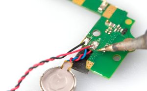
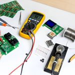
Having the correct tools is essential for safe and reliable PCB Repair. A typical repair workstation may include:
- Soldering iron: A temperature-controlled soldering iron is used to heat solder, PCB pads, wires, and components during repair.
- Multimeter: A multimeter is essential for checking continuity and verifying the repaired circuit before and after repair.
- Magnifying glass or microscope: These tools help identify fine traces, damaged pads, solder bridges, and other small defects.
- Fiberglass pen or scraping tool: These tools can carefully remove solder mask from the copper trace so that a repair connection can be made.
- Jumper wire: Insulated jumper wire can bridge a broken trace and restore electrical continuity while reducing the risk of accidental contact with neighboring conductors.
- Flux and solder: Flux helps remove oxidation and improve solder wetting during the repair process.
- Epoxy or PCB repair coating: Protective materials can mechanically secure a repaired trace and provide additional environmental protection.
The specific tools required depend on the PCB structure, trace width, damage location, and electrical requirements.
How to Repair a Broken PCB Trace
There are several approaches to repairing a damaged PCB trace. Two commonly used methods are jumper-wire repair and trace reconstruction using conductive material and mechanical reinforcement.
1. Jumper Wire Method
The jumper-wire method is practical when a trace has been broken but the surrounding PCB material and connection points remain usable.
Follow these steps:
- Confirm the damaged trace. Use visual inspection and a multimeter to identify the exact location of the open circuit.
- Expose the copper. Carefully remove a small amount of solder mask from both sides of the damaged section using a fiberglass pen or suitable scraping tool.
- Apply flux and tin the exposed copper. Apply a small amount of flux and solder to improve the connection between the exposed copper and jumper wire.
- Prepare the jumper wire. Strip only the necessary length of insulation and tin the exposed conductor.
- Solder one end of the jumper wire. Carefully attach the wire to the exposed copper on one side of the broken trace.
- Solder the other end. Connect the other end of the jumper wire to the corresponding exposed copper area or suitable test point.
- Secure the repair. After confirming that the electrical connection is correct, use PCB-safe solder mask, epoxy, or another suitable protective material to mechanically secure the wire.
- Test the repaired circuit. Use a multimeter to verify continuity and ensure that no accidental short circuit has been introduced.
For low-frequency and relatively simple circuits, a properly installed jumper wire can provide an effective repair. However, high-speed, RF, differential, or controlled-impedance traces may require a more carefully engineered repair because a conventional wire can alter impedance and signal behavior.
2. Trace Reconstruction and Epoxy Reinforcement
A second approach involves reconstructing the damaged trace and mechanically reinforcing the repaired area.
A typical procedure includes:
- Clean the damaged area. Remove dirt, oxidation, flux residue, and other contaminants using an appropriate PCB-safe cleaning method.
- Prepare the damaged copper. Carefully remove damaged or loose material without unnecessarily enlarging the affected area.
- Remove excess solder. Clean existing solder residue around the repair area so the new connection can be accurately positioned.
- Expose and tin the connection area. Apply flux and a small amount of solder to the appropriate copper surfaces.
- Position the replacement conductor. Align the replacement copper strip or fine wire with the original trace path.
- Secure the conductor temporarily. Anti-static tape or another suitable temporary fixture can help hold the conductor in place during soldering.
- Solder the connection. Carefully solder the replacement conductor to the prepared copper areas.
- Apply epoxy reinforcement. Once the electrical connection has been verified, apply a suitable PCB-safe epoxy to mechanically reinforce the repaired section.
- Allow the epoxy to cure. Follow the manufacturer’s curing requirements before applying mechanical stress to the repaired area.
- Perform final testing. Use a multimeter or other appropriate PCB Testing method to verify continuity and confirm that the repair has not created a short circuit.
This approach can be useful when additional mechanical reinforcement is required. However, the repair method should always be selected according to the PCB’s construction, electrical requirements, operating environment, and reliability requirements.
Guidelines for Repairing PCB Traces
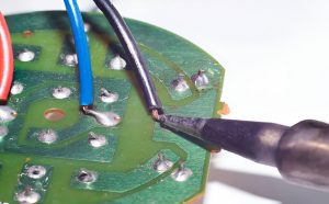
Proper technique is essential when performing PCB Trace Repair. The following guidelines can help improve repair quality and reduce the risk of additional damage.
Match the Electrical Requirements
The replacement conductor should be capable of handling the required current. Its effective cross-sectional area should be appropriate for the original trace and application.
For high-current circuits, simply using a very thin jumper wire may introduce excessive resistance and heating. The repair should therefore be evaluated based on current, temperature rise, voltage, and mechanical requirements.
Avoid Excessive Heat
Excessive soldering temperature or prolonged heating can damage:
- PCB pads
- Copper traces
- Solder mask
- Component leads
- Nearby components
- Internal PCB structures
Use an appropriate soldering temperature and minimize contact time while ensuring adequate solder wetting.
Protect Adjacent Traces
Modern PCBs often contain extremely narrow trace spacing. When removing solder mask or damaged copper, avoid scratching or cutting neighboring traces.
Accidentally connecting adjacent conductors can create a short circuit and introduce a new failure.
Train Repair Personnel
Successful PCB Rework requires appropriate technical knowledge and practical experience. Personnel should understand soldering techniques, ESD protection, PCB construction, component sensitivity, and basic electrical testing before performing repairs on valuable or production boards.
Consider the PCB Layer Structure
A visible surface trace is relatively straightforward to repair. However, damage involving internal layers, buried vias, microvias, or multilayer structures can be significantly more complicated.
If the internal structure has been seriously damaged, replacing the PCB may be more reliable and economical than attempting an extensive repair.
Consider High-Speed and RF Requirements
Not every trace can be repaired using a simple jumper wire.
High-speed differential pairs, RF traces, controlled-impedance transmission lines, and sensitive analog circuits may require controlled geometry and material characteristics. A repair that restores DC continuity may still affect signal integrity.
For these applications, the repair should be evaluated against the original PCB Design requirements.
When Should a PCB Be Repaired or Replaced?
PCB trace repair can be a cost-effective option when the damage is localized and the board remains structurally sound. However, repair is not always the best technical solution.
Replacement may be more appropriate when:
- Multiple internal layers are damaged.
- The PCB substrate is severely cracked or burned.
- Critical pads or vias have been extensively damaged.
- The board is used in a high-reliability application.
- The repair would significantly change controlled-impedance characteristics.
- The cost and risk of repair approach the cost of a replacement PCB.
For production environments, recurring trace failures may also indicate a broader PCB Manufacturing or PCB Design issue. In such cases, repairing individual boards may address the immediate symptom without eliminating the underlying cause.
Conclusion
Repairing a broken PCB trace is an important PCB Repair and PCB Rework technique that can restore electrical continuity without immediately replacing the entire board. The general process involves accurately diagnosing the fault, exposing the damaged copper, creating a reliable electrical connection, mechanically protecting the repair, and performing final PCB Testing.
For simple damaged traces, a carefully installed jumper wire may provide an effective solution. More complex boards may require trace reconstruction, specialized inspection, or professional repair. High-speed, RF, multilayer, and high-reliability applications require additional consideration because restoring continuity alone does not necessarily restore the original electrical performance.
When recurring PCB failures are associated with manufacturing or design issues, working with an experienced PCB manufacturer can help identify the underlying problem and improve future board reliability. Kingda can support customers with professional PCB-related manufacturing and technical services for applications requiring reliable and manufacturable circuit-board solutions.