How to Make a PCB: PCB Design, PCB Manufacturing & PCB Board Manufacturing Guide
Technology is advancing at an unprecedented pace, bringing significant changes to the way people communicate, work, travel, and interact with the world. Smartphones are one of the clearest examples. With just a few taps and swipes, users can send messages, stream music, navigate, take photographs, and access countless applications.
Behind these increasingly compact and powerful devices are numerous electronic components responsible for sensing, monitoring, controlling, processing, imaging, and communication. These components are mounted on or electrically connected to Printed Circuit Boards (PCBs).
A PCB provides the physical and electrical foundation that allows electronic components to work together. However, producing a reliable circuit board involves much more than simply placing copper traces on a substrate. The process includes PCB Design, material selection, imaging, etching, lamination, drilling, plating, solder mask application, surface finishing, inspection, and testing.
This guide explains what a PCB is, the major types of PCBs, how to make a PCB, and the common manufacturing problems that engineers and manufacturers need to control.
What Is a PCB?
A Printed Circuit Board (PCB) is an electronic substrate that mechanically supports components and provides conductive paths for electrical signals and power.
These conductive paths, commonly called traces, are formed from copper. Components are connected to the PCB through solder pads, vias, plated holes, and other conductive features.
A PCB can contain one or multiple copper layers separated by dielectric materials. Depending on the application, it may be rigid, flexible, or a combination of both.
A successful PCB Design must consider multiple engineering factors, including:
- Electrical connectivity
- Signal integrity
- Power distribution
- Thermal management
- Electromagnetic compatibility (EMC)
- Electromagnetic interference (EMI)
- Mechanical constraints
- Component placement
- Manufacturing tolerances
- Assembly requirements
These design considerations directly affect how easily and reliably the board can be manufactured.
What Are the Different Types of PCBs?
PCBs can be classified according to their number of conductive layers, mechanical construction, substrate material, and intended application.
Single-Sided PCB
A single-sided PCB contains one conductive copper layer. Components and conductive features are primarily located on one side of the board.
Because its structure is relatively simple, this type of PCB is suitable for cost-sensitive and less complex electronic products.
Typical applications include basic consumer electronics, simple control circuits, and low-density electronic devices.
Double-Sided PCB
A double-sided PCB contains copper layers on both sides of the substrate.
The two conductive layers can be interconnected through plated through-holes and vias, allowing engineers to create more complex routing than is possible with a single-sided board.
Double-sided PCBs are widely used in industrial controls, consumer electronics, power equipment, and other applications requiring greater circuit density.
Multilayer PCB
A multilayer PCB contains three or more conductive layers separated by dielectric materials.
Internal copper layers can be used for power distribution, ground planes, high-speed signal routing, and other electrical functions. Vias and other interconnection structures connect different layers.
Multilayer construction allows engineers to achieve greater circuit density without significantly increasing the physical size of the board.
Rigid PCB
A rigid PCB uses a mechanically stable substrate, commonly based on materials such as FR-4.
The board maintains its designed shape during normal operation and can be manufactured in single-sided, double-sided, or multilayer configurations.
Rigid PCBs are widely used in computers, industrial equipment, automotive electronics, communication systems, and consumer products.
Flexible PCB
A flexible PCB uses a flexible polymer substrate and thin copper conductors.
Unlike conventional rigid boards, flexible circuits can bend or fold, allowing them to fit into compact or three-dimensional product structures.
Flexible PCBs are commonly used in smartphones, wearable devices, cameras, medical electronics, and other space-constrained products.
Rigid-Flex PCB
A rigid-flex PCB combines rigid and flexible sections within one integrated circuit structure.
This configuration provides the mechanical stability needed for component mounting while allowing selected areas of the board to bend.
Rigid-flex construction can reduce the number of connectors and separate interconnections required in complex three-dimensional electronic assemblies.
How to Make a PCB?
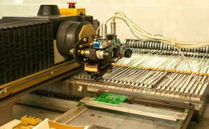
The PCB Manufacturing Process consists of multiple carefully controlled stages. The exact process varies according to the board type, layer count, material, feature size, and performance requirements.
The major stages are described below.
1. PCB Design: Schematic and Layout
The first stage is PCB Design.
Engineers begin by creating a schematic that defines the electrical relationships between components. Symbols, nets, component references, and electrical connections are represented using Electronic Design Automation (EDA) software.
The schematic acts as the electrical blueprint for the board.
The next step is PCB layout. During layout, engineers determine the physical positions of components, traces, vias, pads, copper planes, and other features.
A manufacturing-ready design should also undergo design-rule checking (DRC), signal-integrity analysis where necessary, and Design for Manufacturability (DFM) review.
The final design data is then prepared for manufacturing, commonly including Gerber or other fabrication data, drill files, stackup information, fabrication notes, and relevant assembly documentation.
2. Core and Inner-Layer Fabrication
For a multilayer PCB, the manufacturing process begins with copper-clad core materials and the fabrication of the inner layers.
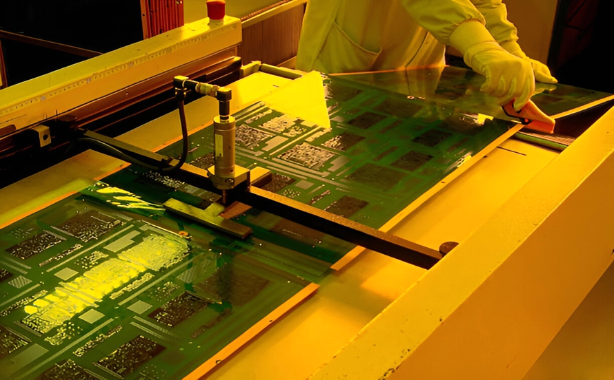
A photoresist is applied to the copper surface. The required circuit pattern is then transferred using an imaging process such as photolithography or direct imaging.
After exposure and development, unwanted copper is removed through chemical etching.
The remaining copper forms the required inner-layer circuitry.
This stage is especially important for multilayer PCB Manufacturing, because defects in internal layers may become inaccessible after lamination.
3. Lamination
Once the inner-layer circuits have been fabricated and inspected, the individual layers are assembled into a multilayer structure.
Core materials and prepreg are stacked according to the specified PCB stackup.
Prepreg contains partially cured resin that bonds the different layers together during lamination.
The stack is placed into a controlled lamination press, where heat and pressure cause the resin to flow and cure.
After cooling, the result is a solid multilayer PCB panel.
Lamination parameters such as temperature, pressure, heating rate, curing time, and material configuration must be carefully controlled to minimize issues such as voids, delamination, and dimensional instability.
4. Drilling
After lamination, holes are drilled according to the fabrication data.
Computer-controlled drilling equipment is used to create through-holes and other required openings.
For advanced high-density designs, laser drilling may be used to create microvias with much smaller dimensions than conventional mechanically drilled holes.
Drilling accuracy is critical because hole position affects layer-to-layer connectivity, component lead alignment, and the reliability of plated through-hole structures.
5. Copper Plating and Outer-Layer Fabrication
After drilling, the exposed hole walls need to become electrically conductive so that different PCB layers can be interconnected.
The board therefore undergoes processes that deposit copper onto the hole walls and surface.
Additional copper plating can then build the required copper thickness.
The outer-layer circuit pattern is subsequently formed using imaging, development, etching, and related processes.
The result is the finished external copper circuitry, including traces, pads, planes, and other conductive structures.
6. Solder Mask Application
Copper traces are susceptible to environmental exposure and accidental solder contact, so a protective solder mask is applied to most of the PCB surface.
The PCB Solder Mask normally covers the copper traces while leaving component pads, selected test points, and other solderable areas exposed.
Modern solder mask materials are commonly applied using processes such as Liquid Photoimageable (LPI) solder mask technology.
The board is coated, exposed, developed, and cured to create accurately defined openings.
A properly processed solder mask helps:
- Protect copper from oxidation and contamination
- Electrically isolate adjacent conductors
- Reduce accidental solder bridging
- Improve PCB assembly consistency
- Protect the board surface
7. Silkscreen Printing
The silkscreen layer provides useful identification and assembly information.
It may include:
- Component reference designators
- Polarity indicators
- Connector labels
- Product information
- Assembly instructions
- Revision information
- Manufacturing or traceability markings
Depending on the manufacturing process, PCB legends can be produced using traditional screen printing, photoimageable processes, or direct legend printing.
Clear and accurate silkscreen information can make PCB assembly, inspection, repair, and maintenance easier.
8. PCB Surface Finish
Before components are assembled, exposed copper pads generally require an appropriate surface finish.
The primary purposes of a PCB Surface Finish are to protect exposed copper and provide a suitable surface for soldering.
Common surface finishes include:
- ENIG (Electroless Nickel Immersion Gold)
- HASL (Hot Air Solder Leveling)
- OSP (Organic Solderability Preservative)
- Immersion tin
- Immersion silver
- ENEPIG for selected advanced applications
The appropriate finish depends on factors such as component pitch, shelf life, soldering process, electrical requirements, environmental conditions, and cost.
What Are Common PCB Manufacturing Problems?
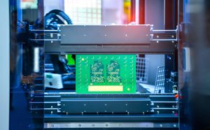
Even with a well-developed PCB Manufacturing Process, defects can occur if design, materials, equipment, or process parameters are not properly controlled.
Understanding these potential problems is essential for producing reliable PCBs.
Design-Related Problems
Some manufacturing problems originate before the board reaches the factory.
For example, insufficient spacing between traces and pads can increase the risk of electrical shorts or inadequate insulation.
Poor thermal design can also create excessive heat around components or prevent efficient heat dissipation.
DFM analysis should therefore be performed before manufacturing begins.
A robust design review can identify problems involving:
- Trace width
- Trace spacing
- Hole sizes
- Pad geometry
- Component clearance
- Copper balance
- Thermal management
- Manufacturing tolerances
- Assembly constraints
Design iterations and prototype testing can then reduce the risk of expensive production changes.
Plating Problems
Copper plating must be carefully controlled because insufficient or uneven plating can affect electrical and mechanical reliability.
Potential problems include:
- Voids in plated holes
- Insufficient copper thickness
- Uneven plating
- Poor adhesion
- Excessive plating
- Plating defects around drilled holes
Manufacturers monitor chemical conditions, current density, temperature, plating time, equipment condition, and other parameters to maintain consistent results.
Delamination
Delamination occurs when layers within the PCB structure separate or lose adequate adhesion.
Thermal expansion, moisture, material compatibility, excessive thermal stress, and improper lamination conditions can contribute to this type of failure.
Proper material selection, moisture control, and optimized lamination parameters are important for preventing delamination.
PCB Warpage
PCB warpage occurs when the board deviates from its intended flat shape.
Differences in thermal expansion between materials, uneven copper distribution, asymmetric stackups, and thermal processing can contribute to warpage.
Excessive warpage can create difficulties during component placement and soldering.
Engineers can reduce the risk by considering:
- Symmetrical stackup design
- Balanced copper distribution
- Appropriate material selection
- Controlled lamination
- Proper thermal processing
Drilling Defects
Drilling is one of the most important mechanical processes in PCB production.
Potential drilling defects include:
- Hole misalignment
- Burrs
- Rough hole walls
- Incorrect hole diameter
- Excessive hole-wall damage
- Resin smear
Hole misalignment can affect electrical connections and component lead insertion. Rough or damaged hole walls can also compromise plated through-hole reliability.
Proper tool selection, drilling parameters, tool condition, and process control are therefore essential.
How PCB Design Affects PCB Manufacturing
The relationship between PCB Design and PCB Manufacturing is critical.
A board may be electrically functional in theory but still be difficult or expensive to manufacture if the design ignores manufacturing constraints.
Design engineers should consider manufacturing requirements from the beginning rather than treating manufacturing as a separate final step.
Important considerations include:
Trace Width and Spacing
Trace width and spacing must match the electrical requirements and manufacturing capabilities.
High-density designs may require finer features, but unnecessarily aggressive geometries can increase manufacturing complexity and cost.
Via and Hole Design
Hole diameter, aspect ratio, via type, and annular ring requirements should be compatible with the selected fabrication process.
Advanced structures such as microvias may be necessary for high-density designs but require more specialized manufacturing processes.
Stackup Design
A properly engineered multilayer stackup supports signal integrity, power distribution, thermal performance, and manufacturability.
The stackup should be developed with the actual PCB materials and manufacturing process in mind.
Design for Manufacturability
DFM checks help identify potential manufacturing problems before production.
A DFM review may examine:
- Minimum trace width
- Minimum spacing
- Drill-to-copper clearance
- Annular rings
- Solder mask openings
- Copper-to-edge clearance
- Layer registration
- Panelization
- Material selection
This approach helps reduce production risks and unnecessary redesigns.
How to Improve PCB Manufacturing Quality
Reliable PCB production requires coordination between design engineers, material suppliers, PCB manufacturers, and assembly teams.
Several practices can improve overall quality:
- Define manufacturing requirements early.
- Use appropriate PCB materials for the operating environment.
- Perform DFM and design-rule checks before fabrication.
- Maintain accurate fabrication documentation.
- Control drilling, plating, lamination, and imaging parameters.
- Use appropriate solder mask and surface finish materials.
- Inspect inner and outer layers throughout production.
- Perform electrical testing on finished boards when required.
- Monitor process data and identify recurring defects.
- Work with a PCB manufacturer experienced in the required technology.
Conclusion
Understanding how to make a PCB requires more than knowing how copper traces are formed. A reliable board is the result of coordinated PCB Design, material selection, fabrication, lamination, drilling, plating, solder mask application, surface finishing, inspection, and testing.
The manufacturing route also depends heavily on the type of PCB being produced. Single-sided, double-sided, multilayer, rigid, flexible, and rigid-flex PCBs each require different material and process considerations.
For engineers, one of the most important principles is to connect PCB Design decisions with manufacturing capabilities from the beginning. Appropriate trace dimensions, hole structures, stackup configuration, copper distribution, solder mask clearances, and surface finishes can significantly improve manufacturability and reliability.
For manufacturers, stable process control and systematic inspection are equally important. By combining sound design practices with a controlled PCB Manufacturing Process, companies can reduce defects, improve production consistency, and produce circuit boards that meet the electrical, mechanical, and reliability requirements of modern electronic products.
Kingda can support PCB projects from fabrication requirements through manufacturing considerations, helping customers develop practical and manufacturable PCB solutions for different electronic applications.