What Is a PCB in Electronics? PCB Design, PCB Manufacturing & PCB Types Guide
The potential breakthroughs enabled by modern electronics are unprecedented. From ultra-thin smartphones and compact storage devices to autonomous vehicles and intelligent industrial systems, electronic technology has transformed ideas that once seemed impossible into practical products.
Behind these innovations are countless electronic components and the printed circuit boards (PCBs) that connect and support them. Components perform functions such as sensing, monitoring, processing, controlling, communication, imaging, and power management, while the PCB provides the electrical and mechanical infrastructure that allows these components to work together.
A PCB is therefore much more than a piece of material with copper traces. Its layer structure, substrate, copper distribution, vias, solder mask, surface finish, and manufacturing tolerances all affect the performance and reliability of the final electronic product.
This article explains what a PCB is in electronics, the major types of PCBs, the different layers that make up a circuit board, and the major steps involved in PCB Manufacturing.
What Is a Printed Circuit Board?
A Printed Circuit Board (PCB) is a structural platform used to mechanically support electronic components and electrically connect them through conductive patterns.
Copper traces, pads, planes, and vias form the conductive network that allows electrical signals and power to move between components.
A typical PCB may contain:
- Copper conductors
- Dielectric materials
- Component pads
- Vias and plated holes
- Solder mask
- Silkscreen
- Surface finish
The complexity of the board depends on its intended application. A simple single-sided PCB may contain only one copper layer, while advanced multilayer PCBs can contain numerous conductive and dielectric layers.
Modern PCB technology is widely used in automotive electronics, telecommunications, industrial automation, consumer electronics, medical devices, IoT equipment, AI hardware, and computing systems.
As electronic products become smaller and more powerful, engineers increasingly rely on advanced PCB Design techniques to achieve higher circuit density, better signal integrity, improved thermal management, and reliable power distribution.
What Are the Different Types of PCBs?
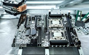
PCBs can be classified in several ways. Two of the most common classification methods are the number of conductive layers and the type of substrate or mechanical construction.
PCB Types Based on Number of Layers
The number of conductive layers directly affects routing density, electrical performance, manufacturing complexity, and cost.
1. Single-Sided PCB
A single-sided PCB contains one conductive copper layer.
Components are generally mounted on one side, while the copper circuitry is formed on the opposite or designated conductive surface.
Because the structure is relatively simple, single-sided PCBs are often used in cost-sensitive and low-complexity products such as basic control circuits, calculators, simple power supplies, and household electronics.
2. Double-Sided PCB
A double-sided PCB contains copper layers on both sides of the dielectric substrate.
Vias and plated through-holes can electrically connect the two conductive layers, allowing engineers to route more complex circuits within a relatively compact board area.
Double-sided PCBs are widely used in consumer electronics, industrial equipment, power electronics, automotive systems, and embedded devices.
3. Multilayer PCB
A multilayer PCB contains three or more conductive layers separated by dielectric materials.
Internal layers can be used for signal routing, power distribution, ground planes, and other electrical functions.
Vias provide connections between different layers, allowing engineers to achieve high routing density without making the board excessively large.
Multilayer construction is particularly important for modern high-speed and high-density products where electrical performance and space utilization are critical.
PCB Types Based on Substrate and Construction
1. Rigid PCB
A rigid PCB uses a mechanically stable substrate, such as FR-4, that maintains its shape during normal operation.
Rigid boards are among the most widely used PCB types and are found in automotive electronics, computers, industrial controls, consumer electronics, communication equipment, and many other products.
2. Flexible PCB
A flexible PCB uses a flexible substrate, commonly polyimide, together with thin copper conductors.
Unlike rigid boards, flexible circuits can bend, fold, or conform to three-dimensional product structures.
Flexible PCBs are especially useful in smartphones, wearable electronics, cameras, medical devices, and other compact products where space is limited.
3. Rigid-Flex PCB
A rigid-flex PCB combines rigid and flexible sections into a single integrated circuit structure.
The rigid portions provide mechanical support for components, while the flexible sections allow the circuit to bend or conform to complex shapes.
Rigid-flex technology is used in applications such as aerospace systems, medical equipment, advanced consumer electronics, and other products where space, weight, and interconnection reliability are important.
What Are the Different Layers of a PCB?
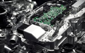
Understanding PCB layer construction is essential for both PCB Design and PCB Manufacturing.
A PCB’s exact structure varies according to its layer count and application, but common layers include dielectric materials, copper layers, solder mask, silkscreen, and surface finishes.
1. Dielectric Layers
Dielectric materials electrically isolate adjacent copper layers while providing mechanical support.
FR-4 is one of the most widely used PCB substrate materials. It is a glass-reinforced epoxy laminate that offers a useful combination of mechanical strength, electrical insulation, thermal performance, and manufacturability.
In multilayer PCBs, dielectric structures commonly include core materials and prepreg.
Core
A core is a fully cured laminate containing dielectric material and copper foil.
In a typical multilayer PCB, copper layers are bonded to the dielectric core and patterned to form the required circuitry.
Prepreg
Prepreg is a partially cured resin-and-glass material used to bond PCB layers together during lamination.
When heat and pressure are applied, the resin flows and cures, creating a mechanically stable multilayer structure.
The selection of dielectric materials and prepreg thickness affects impedance, capacitance, dielectric spacing, thermal performance, and overall stackup characteristics.
2. Copper Layers
Copper layers form the primary conductive structures of a PCB.
Depending on the design, copper can be used for:
- Signal traces
- Ground planes
- Power planes
- Component pads
- Vias
- Thermal structures
In a multilayer PCB, external copper layers are often used for component connections and routing, while internal copper layers can provide high-speed signal paths, power distribution, and reference planes.
Copper thickness must be selected according to current requirements, thermal considerations, mechanical requirements, and manufacturing capabilities.
3. Solder Mask
The PCB Solder Mask is a protective coating applied over most of the copper surface.
It normally leaves component pads and other designated solderable areas exposed.
The solder mask helps:
- Protect copper from environmental exposure
- Reduce oxidation and contamination
- Electrically isolate adjacent conductors
- Reduce solder bridging
- Improve PCB assembly consistency
Green is the most familiar solder mask color, although black, blue, red, white, yellow, purple, and other colors are also available.
4. Silkscreen
The silkscreen, also called the legend layer, provides visual information about the PCB.
It may include:
- Component reference designators
- Polarity indicators
- Connector labels
- Product information
- Revision markings
- Assembly instructions
- Identification codes
Clear silkscreen information can make assembly, inspection, troubleshooting, and maintenance easier.
5. Surface Finish
Exposed copper pads require an appropriate PCB Surface Finish to protect the copper and maintain solderability.
Common surface finishes include:
- HASL (Hot Air Solder Leveling)
- ENIG (Electroless Nickel Immersion Gold)
- OSP (Organic Solderability Preservative)
- Immersion tin
- Immersion silver
- ENEPIG
The appropriate finish depends on component pitch, soldering requirements, shelf-life expectations, electrical requirements, environmental conditions, and project cost.
How Are Printed Circuit Boards Manufactured?
The PCB Manufacturing Process involves multiple stages. The exact sequence varies depending on whether the board is single-sided, double-sided, multilayer, rigid, flexible, or rigid-flex.
The following overview uses a simplified PCB fabrication flow to explain the major principles.
1. PCB Schematic and Layout
The process begins with PCB Design.
Engineers first develop the schematic to define the electrical relationships between components.
EDA software is then used to create the physical PCB layout, including:
- Component placement
- Trace routing
- Via locations
- Copper planes
- Board outline
- Mounting holes
- Clearance requirements
Before fabrication, the design should undergo design-rule checking and DFM analysis to ensure that the PCB can be manufactured reliably.
Manufacturing data is then generated according to the selected fabrication process.
2. Panel Preparation
PCB manufacturers commonly arrange multiple individual boards onto a larger production panel.
Panelization improves material utilization and production efficiency and can make manufacturing and assembly easier.
The panel may include features such as:
- V-score
- Tab routing
- Tooling holes
- Fiducial marks
- Breakaway tabs
After manufacturing and assembly, individual boards can be separated from the panel.
3. Copper Pattern Formation and Etching
For many PCB fabrication processes, unwanted copper is removed through controlled chemical etching.
A protective imaging or photoresist process defines which copper areas should remain.
The exposed copper is then removed by an etching solution, leaving the desired conductive pattern.
Etching accuracy is critical because excessive or insufficient etching can affect trace width, spacing, impedance, and electrical reliability.
4. PCB Drilling
Holes are created according to the PCB fabrication data.
Mechanical drilling is commonly used for standard through-holes and other larger openings.
Laser drilling can be used for smaller structures such as microvias in high-density PCB applications.
Drilling must be accurately controlled because hole position and diameter directly affect interlayer connections, component mounting, and plated-hole reliability.
5. Copper Plating
For boards requiring plated through-holes or other interlayer connections, copper is deposited onto the drilled hole walls.
The conductive hole walls create electrical paths between different copper layers.
Copper plating is particularly important for multilayer PCBs because it allows signals and power to travel between internal and external layers.
Plating thickness and uniformity must be controlled carefully to ensure reliable electrical and mechanical performance.
6. Solder Mask
After the primary copper circuitry has been formed, a solder mask is applied.
The solder mask protects the copper traces and leaves selected pads exposed for component soldering.
Modern LPI solder mask processes can provide accurate openings for increasingly dense PCB designs.
7. Surface Finishing
The exposed pads receive the selected surface finish.
The finish protects the underlying copper and provides an appropriate solderable surface during PCB assembly.
For fine-pitch components, surface-finish selection can be particularly important because pad flatness, solderability, and surface condition can influence assembly quality.
8. Electrical Testing
Before shipment, fabricated PCBs may undergo electrical testing to identify open circuits, short circuits, or other connectivity problems.
Two common methods are:
Flying Probe Testing
Flying probe systems use movable test probes to contact selected test points on the PCB.
Because the probes can move between different locations, this method is flexible and is often useful for prototypes and lower-volume production.
In-Circuit Testing
ICT uses a dedicated fixture containing multiple spring-loaded probes, often called a bed-of-nails fixture.
The fixture can contact predetermined test points and evaluate electrical characteristics according to the test program.
ICT can be efficient for high-volume production when a suitable test fixture is available.
What Factors Affect PCB Manufacturing Quality?
A reliable PCB Manufacturing Process requires careful control of materials, equipment, process parameters, and design data.
Several factors can have a significant impact on the final board.
Design Rules
Trace width, spacing, hole size, annular ring, solder mask clearance, and other geometries must be compatible with the selected manufacturing process.
Designs that push manufacturing capabilities too aggressively may increase fabrication difficulty and defect risk.
Material Selection
The substrate should be selected according to electrical, thermal, mechanical, and environmental requirements.
For example, high-speed designs may require controlled dielectric properties, while high-temperature applications may require materials with appropriate thermal stability.
Stackup Configuration
A well-designed multilayer stackup can improve signal integrity, power distribution, impedance control, and EMI performance.
The stackup should be developed together with the PCB manufacturer’s available materials and fabrication capabilities.
Copper Distribution
Uneven copper distribution can contribute to warpage and dimensional instability during thermal processing.
Balanced copper distribution is therefore an important consideration in multilayer PCB Design.
Manufacturing Tolerances
PCB dimensions, hole sizes, layer registration, copper thickness, solder mask openings, and other features have manufacturing tolerances.
Understanding these tolerances during design helps prevent conflicts between the intended design and the actual fabrication process.
Why Are PCBs Important in Modern Electronics?
PCBs are fundamental to almost every category of electronic equipment.
Consumer Electronics
Smartphones, laptops, tablets, televisions, cameras, and gaming systems all depend on PCBs to connect their electronic components.
Automotive Electronics
Modern vehicles contain numerous electronic control units and systems for power management, infotainment, sensing, safety, communication, and driver assistance.
IoT Devices
IoT products require compact PCBs to integrate processors, sensors, wireless communication modules, power-management circuits, and other components.
AI and Computing Hardware
AI systems and high-performance computing equipment require advanced PCB technologies to handle high-speed signals, high power density, thermal requirements, and complex interconnections.
Industrial Electronics
Industrial automation, robotics, control systems, instrumentation, and communication equipment rely heavily on reliable PCB assemblies.
Conclusion
A Printed Circuit Board (PCB) is the electrical and mechanical foundation of modern electronic products. It connects components, distributes power, routes signals, provides mechanical support, and enables increasingly sophisticated electronic functions.
PCBs can be classified by conductive layer count and construction, including single-sided, double-sided, multilayer, rigid, flexible, and rigid-flex designs. Each type provides different capabilities and is selected according to the electrical, mechanical, thermal, and spatial requirements of the final product.
Understanding PCB construction is equally important. Dielectric layers provide insulation and mechanical support, copper layers form conductive paths, solder mask protects the circuitry, silkscreen provides identification information, and surface finishes protect exposed copper pads and support reliable soldering.
From schematic development and layout to panelization, etching, drilling, plating, solder mask application, surface finishing, and electrical testing, every stage of PCB Manufacturing contributes to the quality and reliability of the final board.
For engineers developing new electronic products, effective PCB Design should always take manufacturing capabilities into account. Working with an experienced PCB manufacturing partner can help ensure that the selected materials, stackup, fabrication process, and quality controls are appropriate for the intended application.
Kingda can support PCB projects with manufacturing-oriented engineering considerations, helping customers develop practical PCB solutions for consumer electronics, industrial equipment, automotive systems, communications, and other electronic applications.