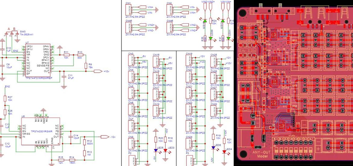
How to Convert a Schematic to PCB Layout: PCB Design, PCB Manufacturing & Layout Guide
Every electronic product begins with an initial concept, schematic design, and prototype development. Product requirements and user needs are first translated into a logical circuit schematic and supporting design data. A schematic is a symbolic representation of an electronic circuit that defines components such as resistors, capacitors, diodes, transistors, and integrated circuits, as well as their electrical relationships.
However, a schematic alone cannot be manufactured. To turn the circuit concept into a physical product, engineers must convert the schematic into a manufacturable PCB layout. This process transforms the logical electrical connections into physical component footprints, copper traces, vias, layers, board geometry, and manufacturing data.
Modern PCB design software such as Altium Designer, KiCad, Autodesk Fusion/EAGLE, Proteus, and EasyEDA provides tools for schematic capture, component management, PCB placement, routing, simulation, design-rule checking, and manufacturing-data generation.
This guide explains how to convert a circuit schematic into a practical PCB Layout, from schematic preparation and footprint assignment to component placement, routing, DRC, and Gerber generation.
What Is the Difference Between a Schematic and a PCB Layout?
Before converting a schematic into a PCB layout, it is important to understand the difference between these two design representations.
A PCB Schematic describes the electrical function of a circuit. It shows:
- Components
- Electrical connections
- Net names
- Power rails
- Signal paths
- Component reference designators
- Component values
- Pin relationships
- Circuit blocks
A PCB layout, in contrast, describes the physical implementation of that circuit. It defines:
- Component footprints
- Component locations
- Board outline
- Copper layers
- Trace widths
- Trace spacing
- Vias
- Copper pours
- Drill holes
- Keepout areas
- Silkscreen
- Solder mask openings
The schematic answers “What is electrically connected?”, while the PCB layout answers “Where is everything physically located, and how will those connections be manufactured?”
Both representations must remain synchronized throughout the design process.
Steps to Prepare a PCB Layout
Converting a circuit schematic into a PCB layout is one of the most important stages of PCB Design. Errors in component footprints, placement, routing, or electrical connectivity can result in manufacturing problems or a non-functional product.
The following steps provide a practical workflow for converting a schematic into a manufacturable PCB layout.
1. Create and Verify the Circuit Schematic
The first step is to create a complete and logically correct schematic.
The schematic should clearly define all components, electrical connections, power supplies, signal paths, polarity, and circuit blocks.
Before starting the physical layout, engineers should verify:
- Component values
- Reference designators
- Pin assignments
- Power connections
- Ground connections
- Signal connectivity
- Component polarity
- Unconnected pins
- Required protection circuits
- Interface connections
Schematic errors can propagate into the PCB layout, making them more expensive to correct later.
For complex designs, it is useful to divide the schematic into functional blocks such as power management, processing, communication, analog circuits, RF circuits, and interfaces.
2. Assign the Correct Component Footprints
A schematic symbol represents the electrical function of a component, but it does not necessarily define its physical dimensions.
Each component therefore needs an appropriate PCB footprint.
For example, a resistor may use a through-hole axial footprint or a surface-mount package such as 0402, 0603, or 0805. An integrated circuit may require a QFN, QFP, BGA, SOIC, or other package.
Footprint selection should consider:
- Package dimensions
- Pin pitch
- Pad dimensions
- Component height
- Mounting technology
- Manufacturer recommendations
- Assembly process
- PCB fabrication capabilities
An incorrect footprint can result in component placement problems, soldering defects, assembly failures, or even an unusable PCB.
Engineers should use verified footprints whenever possible and compare them with the component manufacturer’s datasheet.
3. Define the PCB Board Outline
The next step is to establish the physical dimensions and shape of the PCB.
The board outline should reflect the mechanical requirements of the final product, including:
- Overall board dimensions
- Mounting holes
- Cutouts
- Slots
- Connectors
- Edge clearances
- Mechanical keepouts
- Component height restrictions
- Enclosure constraints
Mechanical requirements should be considered early rather than after routing is completed.
For products with strict size limitations, the PCB must fit within the available enclosure while still providing sufficient space for components, routing, thermal management, testing, and assembly.
For mass production, panelization may also be considered. Multiple PCB units can be arranged into a manufacturing panel to improve production efficiency and reduce handling requirements.
4. Plan the PCB Stackup
For a simple single-sided or two-layer board, stackup planning may be relatively straightforward. However, high-speed, high-density, and multilayer designs require careful stackup planning.
A multilayer PCB may contain:
- Signal layers
- Ground planes
- Power planes
- Core dielectric materials
- Prepreg dielectric layers
- Copper foil
A suitable stackup can help control impedance, reduce electromagnetic interference, improve signal integrity, and provide effective power distribution.
For high-speed interfaces, the designer should consider the relationship between trace width, dielectric thickness, copper thickness, and the dielectric constant of the PCB material.
5. Place Components
Component placement determines much of the subsequent routing quality and manufacturing performance.
Components should not simply be placed wherever there is available space. Their locations should reflect electrical, mechanical, thermal, and manufacturing requirements.
Important placement considerations include:
- Functional grouping
- Signal-flow direction
- Component orientation
- Polarity
- Connector locations
- Decoupling capacitor placement
- Thermal requirements
- Component clearance
- Assembly accessibility
- Test access
For example, decoupling capacitors should generally be placed close to the corresponding power pins to minimize the current-loop area.
High-speed components should also be positioned to minimize unnecessary trace length and discontinuities.
Power components may require additional copper area and thermal management, while heat-generating devices should be positioned where heat can be effectively dissipated.
6. Route PCB Traces
After component placement, electrical connections are converted into physical copper traces.
Routing is one of the most important stages of PCB Design because trace geometry can affect signal integrity, power delivery, electromagnetic compatibility, and manufacturability.
Key routing parameters include:
- Trace width
- Trace spacing
- Trace length
- Layer transitions
- Via placement
- Differential-pair spacing
- Controlled impedance
- Return-current paths
- Copper thickness
Different signals may require different routing strategies.
For example, high-current power traces generally require greater copper cross-sectional area, while high-speed differential signals require controlled geometry and carefully maintained return paths.
Avoid unnecessary sharp corners, excessive vias, and long signal paths. At the same time, routing should not be optimized only for minimum trace length. Signal integrity and return-current behavior must also be considered.
7. Add Vias and Additional PCB Layers
As circuit complexity increases, a two-layer PCB may not provide enough routing space.
Multilayer PCB technology allows designers to distribute signals and power across several copper layers.
Vias provide electrical connections between different layers. Common types include:
- Through vias
- Blind vias
- Buried vias
- Microvias
Blind and buried vias can provide routing flexibility in high-density designs, while microvias are widely used in HDI PCB technology.
However, additional layers and advanced via structures increase manufacturing complexity and cost. Therefore, layer count should be selected according to electrical, mechanical, manufacturing, and cost requirements rather than simply maximizing density.
8. Add Ground Planes and Copper Areas
Grounding is an important part of PCB layout design.
A continuous ground plane can provide a low-impedance return path and help reduce unwanted loop area. It can also support power distribution and electromagnetic compatibility.
When using copper pours, designers should check:
- Ground connectivity
- Thermal relief settings
- Clearance
- Isolation areas
- Return-current paths
- High-voltage spacing
- Analog/digital partitioning where appropriate
Ground planes should not be divided unnecessarily because poorly planned splits can force return currents to take longer and less predictable paths.
9. Perform Design Rule Checks (DRC)
Once component placement and routing are complete, the PCB layout should undergo a comprehensive Design Rule Check (DRC).
DRC automatically checks the layout against predefined rules and can identify potential problems such as:
- Trace-to-trace clearance violations
- Trace-to-pad clearance violations
- Minimum trace-width violations
- Unconnected nets
- Short circuits
- Incorrect via dimensions
- Board-edge clearance violations
- Silkscreen conflicts
- Manufacturing constraints
However, DRC is not a replacement for engineering review. A layout can pass automated DRC and still contain functional problems.
Engineers should therefore perform a manual review of critical circuits, power paths, high-speed interfaces, component orientation, thermal areas, and mechanical interfaces.
10. Perform Design for Manufacturability (DFM) Review
Before releasing the PCB for fabrication, the design should also be evaluated for manufacturability.
Design for Manufacturing (DFM) helps identify problems that may not be detected by standard electrical design rules.
Typical DFM considerations include:
- Minimum trace width
- Minimum spacing
- Hole size
- Aspect ratio
- Annular ring
- Copper-to-edge clearance
- Solder mask clearance
- Silkscreen clearance
- Surface finish
- Panelization
- Component assembly requirements
The exact manufacturing limits depend on the PCB fabricator and the technology being used.
For this reason, engineers should review the manufacturer’s capabilities before finalizing the design.
11. Generate Gerber and Manufacturing Files
After the layout has passed electrical and manufacturing reviews, the design data can be prepared for fabrication.
Gerber files are widely used to communicate PCB artwork information to manufacturers. Depending on the design and manufacturer, the fabrication package may include:
- Copper layer files
- Solder mask files
- Silkscreen files
- Board outline
- Drill files
- Paste files
- Fabrication drawings
- Stackup information
- Impedance requirements
- Special manufacturing instructions
It is important to understand that a Gerber package is not simply a single file containing the entire PCB. A typical manufacturing data package consists of multiple files representing different PCB layers and manufacturing information.
The exact output requirements should be confirmed with the PCB manufacturer before production.
Key Considerations When Converting a Schematic to PCB Layout
A successful PCB Layout requires more than simply connecting all nets. The following practices can help prevent design and manufacturing problems.
Use Clear Reference Designators
All components should have clear reference designators and documentation. This makes assembly, inspection, testing, troubleshooting, and repair easier.
Keep Critical Traces as Short as Practical
Shorter routing can reduce parasitic effects and signal delay in some circuits. However, routing should also preserve controlled impedance, return paths, and signal-integrity requirements.
Avoid Unnecessary Routing Complexity
Avoid excessive vias, unnecessary layer changes, and unnecessarily long routes. A simpler layout is generally easier to manufacture, inspect, and troubleshoot.
Maintain Adequate Component Spacing
Components should have enough spacing for assembly equipment, soldering, inspection, rework, and thermal management.
Crowded layouts can create solder bridges, component interference, inspection difficulties, and repair problems.
Verify Ground and Power Connectivity
Power and ground networks should be reviewed carefully before manufacturing.
Check that:
- Every required ground connection is present.
- Power planes are correctly connected.
- High-current paths have sufficient copper.
- Analog and digital circuits have appropriate return paths.
- Sensitive signals are not unnecessarily routed through noisy areas.
Check Component Orientation and Polarity
Polarized components must be correctly oriented.
This includes:
- Diodes
- LEDs
- Electrolytic capacitors
- Integrated circuits
- Connectors
- Batteries
- Certain sensors and modules
Incorrect polarity can cause immediate failure or permanent component damage.
Verify Input and Output Interfaces
All connectors and external interfaces should be checked against the product specification.
Confirm:
- Pin assignments
- Connector orientation
- Voltage levels
- Current requirements
- Signal types
- Protection requirements
- Mechanical compatibility
Use Manufacturable Footprints
Footprints should correspond to real, commercially available components and should be suitable for the intended assembly method.
An electrically correct footprint that cannot be reliably assembled is still a poor PCB design.
Common PCB Layout Mistakes
Several common mistakes can create problems during PCB Manufacturing.
Incorrect Footprints
An incorrect footprint may prevent the selected component from fitting or being soldered correctly.
Poor Component Placement
Placing critical components too far apart can create unnecessarily long signal paths and poor power distribution.
Insufficient Clearance
Insufficient spacing between traces, pads, vias, or board edges can create fabrication defects or electrical failures.
Poor Thermal Design
Power devices and heat-generating components may require thermal vias, larger copper areas, heatsinks, or other cooling strategies.
Missing Return Paths
High-speed signals require an appropriate return-current path. Breaking the reference plane beneath a critical signal can increase loop area and electromagnetic interference.
Ignoring Manufacturing Capabilities
A PCB layout may be electrically valid but impossible or expensive to manufacture if it exceeds the fabricator’s capabilities.
PCB Design to PCB Manufacturing Workflow
The conversion from schematic to finished PCB can be viewed as a complete engineering workflow:
Product Requirements → Circuit Schematic → Component Selection → Footprint Assignment → PCB Stackup → Board Outline → Component Placement → Routing → DRC → DFM Review → Gerber/Drill Files → PCB Manufacturing → PCB Assembly → Inspection and Testing
Each stage affects the next. Errors introduced during schematic design can propagate into the layout, while poor layout decisions can increase fabrication and assembly costs.
This is why successful PCB Manufacturing begins well before the fabrication stage.
Conclusion
Converting a circuit schematic into a physical PCB layout is a multidisciplinary engineering process that combines electrical design, mechanical constraints, signal integrity, thermal management, manufacturing requirements, and assembly considerations.
The process begins with a verified schematic and correct component footprints. Engineers then define the board outline, plan the stackup, place components, route traces, add vias and planes, perform DRC and DFM reviews, and finally generate the manufacturing data required for fabrication.
A successful PCB layout should not only function electrically but also be manufacturable, testable, inspectable, and serviceable. By incorporating PCB Design and PCB Manufacturing requirements from the beginning, engineers can reduce design revisions, manufacturing defects, assembly problems, and unnecessary production costs.
For professional PCB projects, manufacturers such as Kingda can be involved early in the development process so that fabrication and assembly capabilities can be considered before the design is released for production.