How to Solder a PCB: PCB Design, PCB Manufacturing & PCB Soldering Guide
Whether you are a DIY electronics enthusiast or an engineer developing complex electronic systems, understanding how to solder a printed circuit board (PCB) is an essential skill. A properly soldered PCB provides reliable electrical and mechanical connections, helping electronic products operate safely and consistently throughout their service life.
However, PCB Soldering involves much more than simply melting solder. It requires the right tools, appropriate temperature control, proper soldering techniques, and careful inspection of every solder joint. This guide explains the fundamentals of PCB soldering, including essential tools, common soldering methods, inspection techniques, safety precautions, rework procedures, and troubleshooting tips.
What Is PCB Soldering?
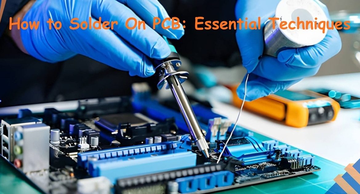
PCB Soldering is the process of using molten solder to create a permanent electrical and mechanical connection between electronic components and a printed circuit board. During the process, component leads or terminals are joined to copper pads on the PCB through a controlled heating and soldering operation.
When the solder melts, it flows across the heated metal surfaces and wets both the component terminal and PCB pad. As the solder cools and solidifies, it forms a conductive joint that mechanically secures the component to the board.
Proper soldering is essential in PCB prototyping, electronics manufacturing, repair, and rework. The quality of each solder joint can directly affect the electrical performance and long-term reliability of the finished product.
Basic Principle of PCB Soldering
The basic soldering process can be summarized as follows:
- Position the component correctly on the PCB.
- Heat the PCB pad and component terminal simultaneously.
- Apply an appropriate amount of solder to the heated joint.
- Allow the solder to flow and wet both surfaces.
- Remove the solder and soldering iron while maintaining component stability.
- Allow the joint to cool naturally.
- Inspect the finished solder joint.
The objective is to create a clean, well-wetted joint without excessive solder, insufficient solder, solder bridges, or thermal damage.
Leaded vs. Lead-Free Solder
Leaded solder alloys generally have lower melting temperatures and can be easier to work with during manual soldering. However, lead-containing materials are subject to environmental and regulatory restrictions in many applications.
Lead-free solder alloys, commonly based on tin with elements such as silver and copper, require higher processing temperatures. They are widely used in modern electronics manufacturing to meet requirements such as RoHS compliance.
The choice of solder should be based on the PCB assembly process, component specifications, product requirements, and applicable regulations.
Applications of PCB Soldering
PCB soldering is used across many industries, including:
- Consumer electronics
- Automotive electronics
- Telecommunications
- Industrial automation
- Medical electronics
- Aerospace and defense
- Renewable energy systems
- IoT devices
- Power electronics
From simple prototype boards to sophisticated multilayer assemblies, reliable solder joints are fundamental to electronic product performance.
Why Proper PCB Soldering Matters
The quality of individual solder joints has a direct impact on the reliability and service life of an electronic assembly. Poor soldering can result in intermittent electrical connections, component failures, signal integrity problems, and expensive rework.
Strong Mechanical Connections
Solder provides both electrical continuity and mechanical attachment between a component and the PCB. Properly formed joints can withstand normal vibration, mechanical stress, and thermal cycling encountered during product operation.
Reduced Product Failures
Many PCB assembly defects originate from soldering problems rather than defective components. Proper process control can reduce defects such as solder bridges, insufficient solder, cold solder joints, cracks, and incomplete wetting.
Improved Manufacturing Quality
A consistent soldering process helps manufacturers improve production yield and reduce rework. In high-volume PCB Manufacturing, repeatability is particularly important because thousands or millions of solder joints may need to meet the same quality requirements.
Reliable Electrical Connections
A properly formed solder joint provides a low-resistance electrical path between the component and PCB conductor. Reliable connections help maintain stable current flow and signal transmission while reducing the risk of intermittent failures.
Essential Tools for PCB Soldering
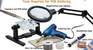
Before learning how to solder a PCB, prepare the appropriate tools and equipment. Good-quality soldering equipment can improve joint consistency, reduce component damage, and make both assembly and repair more efficient.
Temperature-Controlled Soldering Iron
A temperature-controlled soldering iron provides controlled heat for melting solder and forming solder joints. Adjustable temperature control is particularly useful when working with different solder alloys, PCB materials, and temperature-sensitive components.
A suitable soldering tip should also match the size and geometry of the joint. A tip that is too small may transfer heat inefficiently, while an excessively large tip can increase the risk of thermal damage.
Solder Wire
Solder wire is the filler material used to create the connection between the component terminal and PCB pad. Flux-cored solder is commonly used because the integrated flux helps remove surface oxides and improve wetting during soldering.
Flux
Flux removes or chemically reduces surface oxides and improves solder wetting. Additional liquid or gel flux can be particularly useful when soldering fine-pitch components, repairing oxidized boards, or reworking older assemblies.
The appropriate flux type should be selected according to the assembly process and cleaning requirements.
Solder Wick and Desoldering Pump
Solder wick, also called desoldering braid, uses capillary action to remove excess molten solder. A desoldering pump uses suction to remove solder from through-hole joints or PCB pads.
These tools are particularly useful during PCB Repair and rework.
Precision Tweezers and PCB Holder
Precision tweezers help position small surface-mount components accurately. A PCB holder secures the board during soldering and leaves both hands available for controlled component placement and solder application.
Magnification and Lighting
Good lighting and magnification make it easier to identify small solder bridges, insufficient solder, lifted components, and alignment problems.
A magnifying lamp or digital microscope can be especially useful when working with fine-pitch SMT packages.
Recommended Soldering Temperature
The appropriate soldering iron temperature depends on the solder alloy, component, PCB construction, tip geometry, and joint size.
As a general starting point, many manual soldering applications use approximately 315°C–350°C for leaded solder and around 350°C–380°C for common lead-free solder. These are working ranges rather than universal requirements.
The goal should be to transfer enough heat to create proper wetting quickly without unnecessarily overheating the component, PCB pad, or laminate.
Types of PCB Soldering Techniques
The appropriate PCB Assembly method depends on component technology, production volume, board design, and manufacturing requirements.
Four common approaches are manual soldering, reflow soldering, wave soldering, and selective soldering.
1. Manual Soldering
Manual soldering uses a temperature-controlled soldering iron to connect components to PCB pads manually.
It is widely used for:
- Prototypes
- PCB repair
- Rework
- Engineering samples
- Low-volume production
- Component replacement
Its major advantage is flexibility. An operator can solder or repair individual joints without requiring a complete automated production line.
2. Reflow Soldering
Reflow soldering is the standard process for assembling most SMT components.
First, solder paste is deposited onto PCB pads, usually through a stencil. A pick-and-place machine then positions components on the solder paste. The populated PCB enters a reflow oven where the solder paste follows a controlled thermal profile.
The solder melts during the reflow stage and then cools to form permanent solder joints.
Reflow soldering offers high repeatability and is well suited to modern high-density PCB assemblies.
3. Wave Soldering
Wave soldering is primarily used for through-hole components and some mixed-technology assemblies.
The PCB passes over a controlled wave of molten solder, allowing multiple exposed through-hole terminals to be soldered simultaneously. This makes wave soldering suitable for high-volume production.
However, conventional wave soldering is not generally the preferred method for densely populated SMT assemblies.
4. Selective Soldering
Selective soldering is designed to solder specific through-hole joints without exposing the entire PCB to a conventional solder wave.
It is particularly useful for mixed-technology boards containing both SMT and through-hole components. The process can reduce unnecessary thermal exposure to nearby components and already-assembled SMT joints.
PCB Soldering Technique Comparison
| Soldering Method | Best Application | Main Advantages | Limitations |
|---|---|---|---|
| Manual Soldering | Prototyping, repair, rework | Flexible, low equipment cost, suitable for individual joints | Slower and operator-dependent |
| Reflow Soldering | SMT production | High repeatability, automation, excellent for fine-pitch components | Requires solder paste, stencil, and reflow equipment |
| Wave Soldering | Through-hole production | Fast and efficient for high-volume assembly | Less suitable for dense SMT boards |
| Selective Soldering | Mixed SMT/THT assemblies | Precise localized soldering and controlled thermal exposure | Higher equipment and programming requirements |
How to Inspect PCB Solder Joints
After soldering, inspection is essential for verifying electrical and mechanical integrity. A PCB may appear to function correctly while still containing defects that could cause intermittent or long-term failures.
Visual Inspection
Visual inspection is the simplest and most widely used inspection method.
A properly formed solder joint should show good wetting between the solder, component terminal, and PCB pad. The joint should be free from obvious cracks, solder bridges, excessive solder, contamination, and component misalignment.
Inspection requirements can vary depending on component type and applicable acceptance standards.
Automated Optical Inspection (AOI)
Automated optical inspection (AOI) uses cameras and image-processing systems to inspect assembled PCBs.
AOI can detect issues such as:
- Missing components
- Incorrect component placement
- Polarity errors
- Solder bridges
- Insufficient or excessive solder
- Misalignment
- Visible soldering defects
AOI is particularly useful in high-volume PCB Manufacturing because it provides repeatable inspection coverage.
X-Ray Inspection
X-ray inspection is useful for components whose solder joints cannot be directly observed from the outside.
Typical applications include BGA and QFN packages. X-ray inspection can reveal internal conditions such as solder voids, insufficient solder, bridging, and other hidden defects.
Good vs. Defective Solder Joints
A good solder joint should have appropriate solder coverage and good wetting between the component terminal and PCB pad.
Potential defects include:
- Poor wetting
- Cracks
- Solder bridges
- Insufficient solder
- Excessive solder
- Voids
- Component misalignment
- Lifted or damaged pads
A visual appearance alone is not always sufficient to determine reliability, especially for hidden or high-density connections.
IPC Quality Standards
IPC-A-610 provides acceptance criteria for electronic assemblies, while IPC J-STD-001 establishes requirements and practices related to soldered electrical and electronic assemblies.
Manufacturers should use the applicable revision and class requirements for the specific product rather than treating these standards as a universal single acceptance criterion.
PCB Soldering Tips and Best Practices
Good PCB Soldering requires preparation, controlled heat transfer, correct solder application, and careful inspection.
Keep the Soldering Tip Clean
A clean, properly tinned soldering tip transfers heat more efficiently and helps solder flow consistently.
Clean the tip regularly using an appropriate brass wool or damp sponge according to the soldering equipment manufacturer’s recommendations.
Heat the Pad and Component Together
Before applying solder, heat both the PCB pad and component terminal. This allows solder to wet both surfaces and helps create a stronger electrical and mechanical connection.
Simply melting solder onto a cold pad can produce a weak joint because the solder may not properly wet the underlying metal.
Use the Correct Amount of Solder
Too much solder can create bridges between adjacent pads or make inspection difficult. Too little solder may produce inadequate mechanical attachment or incomplete electrical contact.
The correct amount depends on the pad geometry, component lead, solder alloy, and assembly method.
Control Temperature and Contact Time
Higher temperature does not necessarily mean better soldering. Excessive heat or prolonged contact can damage sensitive components, lift copper pads, or contribute to PCB delamination.
Use the lowest practical temperature that provides reliable wetting within an appropriate contact time.
Keep the PCB Clean
Dust, oil, oxidation, and other contaminants can reduce solderability. Clean the PCB using a suitable process before and after soldering when required.
For assemblies using no-clean flux, cleaning requirements should follow the flux manufacturer’s recommendations and the product’s cleanliness specifications.
PCB Soldering Safety Guidelines
PCB soldering involves high temperatures, electrical equipment, and flux fumes. Appropriate safety practices are therefore essential.
Work in a Well-Ventilated Area
Soldering flux can generate fumes that may irritate the eyes and respiratory system. Use adequate ventilation or appropriate local fume extraction to reduce exposure.
Wear Appropriate PPE
Safety glasses can protect the eyes from solder splashes and debris. Additional PPE should be selected according to the soldering process and workplace risk assessment.
Prevent Electrostatic Discharge
Sensitive integrated circuits can be damaged by electrostatic discharge (ESD), even when no visible damage occurs.
Use appropriate ESD controls, such as grounded work surfaces, wrist straps, and ESD-safe tools, when handling sensitive electronic components.
Handle Hot Equipment Carefully
Soldering irons can reach temperatures well above 300°C. Always place the iron in its designated stand when it is not being used and allow equipment to cool before storage or maintenance.
PCB Rework and Repair Process
Even a well-controlled assembly process may require rework because of component defects, soldering errors, or design changes.
A controlled PCB Repair process helps restore board functionality while minimizing the risk of damaging nearby components, pads, traces, or laminate.
1. Remove the Defective Component
Use an appropriate soldering iron, hot-air rework system, or other suitable rework equipment to heat the solder connection evenly.
Avoid excessive mechanical force because it can lift PCB pads or damage nearby traces.
2. Clean the PCB Pads
Use solder wick and appropriate flux to remove excess solder and prepare the pads for the replacement component.
Clean and properly prepared pads improve solder wetting and make component replacement more predictable.
3. Install the Replacement Component
Position the replacement component according to the PCB design documentation, polarity markings, and component orientation.
For fine-pitch devices, verify alignment before completing all solder joints.
4. Inspect and Test the Repaired PCB
After repair, inspect the solder joints under suitable magnification. Check component orientation, solder coverage, and possible solder bridges.
Where appropriate, perform electrical continuity testing and functional testing before returning the PCB to service.
Common PCB Soldering Mistakes
Even experienced technicians can encounter soldering defects. Understanding common failure modes can help improve process control and reduce rework.
Cold Solder Joints
A cold solder joint can occur when the solder does not properly wet the surfaces being joined. Such joints may appear rough or irregular and can produce unreliable electrical connections.
Solder Bridges
A solder bridge is an unintended connection between adjacent pads or terminals. It can create a short circuit and potentially damage components or prevent the PCB from functioning correctly.
Insufficient Solder
Insufficient solder can result in poor mechanical attachment or incomplete electrical contact. The problem can become more serious under vibration, thermal cycling, or repeated mechanical stress.
Excessive Heating
Prolonged or excessive heating can damage components, lift copper pads, or contribute to PCB laminate damage.
Use appropriate temperature settings and minimize unnecessary heating time.
Improper Flux Application
Flux improves solderability, but excessive or inappropriate flux can create cleaning and reliability concerns depending on the flux chemistry.
Use the amount and type recommended for the soldering process.
Skipping Final Inspection
A board should not be considered complete simply because it powers on. Some soldering defects may only appear intermittently or may become failures after thermal or mechanical stress.
Visual inspection, AOI, X-ray inspection, electrical testing, or functional testing should be selected according to the product’s requirements.
Incorrect Component Placement
Incorrect component orientation or alignment can cause electrical problems and mechanical stress.
Before soldering, verify component position, polarity, reference designators, and orientation against the PCB design documentation.
The Relationship Between PCB Design and Soldering Quality
Soldering quality is influenced not only by the assembly process but also by the original PCB Design.
Good PCB design can make components easier to place, solder, inspect, and rework. Important considerations include:
- Appropriate pad dimensions
- Correct component footprints
- Adequate solder mask clearance
- Suitable component spacing
- Proper thermal relief design
- Appropriate via placement
- Accessible test points
- Sufficient copper area
- Suitable component orientation
- Design for manufacturability (DFM)
For fine-pitch and high-density assemblies, these considerations become increasingly important because small layout changes can affect solder paste printing, component placement, thermal distribution, inspection, and rework.
How PCB Manufacturing Affects Soldering Reliability
The quality of the finished assembly also depends on the broader PCB Manufacturing Process.
Factors such as PCB dimensional accuracy, copper thickness, surface finish, solder mask registration, pad quality, drilling accuracy, and cleanliness can all affect solderability.
Common surface finishes include HASL, ENIG, OSP, immersion tin, and immersion silver. The appropriate finish depends on factors such as component pitch, shelf life, environmental requirements, assembly process, and cost.
Therefore, reliable soldering should be considered throughout the complete PCB lifecycle—from PCB Design and material selection to fabrication, assembly, inspection, and final testing.
Conclusion
Reliable PCB Soldering is fundamental to electronics prototyping, manufacturing, repair, and product development. Successful soldering depends on more than simply melting solder. It requires appropriate tools, controlled temperature, proper solder application, good PCB preparation, effective inspection, and consistent process control.
For professional electronic products, soldering quality should also be considered as part of the broader PCB Manufacturing and process. Proper PCB design, suitable materials and surface finishes, controlled assembly processes, and appropriate inspection methods can work together to improve reliability and reduce defects.
For professional PCB fabrication and assembly projects, working with an experienced manufacturing partner such as Kingda can help integrate design-for-manufacturing considerations, PCB fabrication, assembly, inspection, and testing into a controlled production workflow.