PCB Chemicals in PCB Design and PCB Manufacturing: Types, Processes & Safety Guide
As the electronics industry continues to demand higher reliability, greater circuit density, and improved performance, PCB Manufacturing processes have evolved significantly. Modern production increasingly relies on automation, high-yield processes, tighter process control, and more precise equipment. At the same time, advances in both direct and indirect materials have had a major influence on the quality and reliability of finished circuit boards.
Among these materials, chemicals play an essential role. PCB chemicals are used throughout multiple stages of fabrication and assembly, including cleaning, imaging, etching, plating, surface finishing, soldering, and resist processing. When properly selected and controlled, these chemicals help manufacturers achieve accurate circuit patterns, reliable interconnections, good solderability, and long-term PCB performance.
It is important to clarify one terminology issue first: PCB chemicals in this article means chemicals used in printed circuit board production. It does not mean polychlorinated biphenyls, which are a separate class of industrial chemicals and are not synonymous with PCB manufacturing chemicals.
This guide explains what PCB chemicals are, where they are used, why they matter, and what precautions should be followed when handling them during PCB production.
What Are PCB Chemicals?
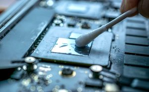
PCB chemicals are chemical compounds, solutions, mixtures, or process additives used during the fabrication and assembly of printed circuit boards. Depending on the manufacturing stage, they may be used for:
- Cleaning and surface preparation
- Photoresist processing
- Copper etching
- Electroless and electrolytic plating
- Solder mask processing
- Surface finishing
- Flux removal
- Contamination control
These chemicals are selected according to the specific manufacturing process, PCB material, required feature geometry, surface finish, and production requirements.
For example, an etchant selectively removes unwanted copper, while a plating solution deposits conductive material onto copper surfaces and plated-through holes. Cleaning chemicals remove organic residues, flux, oils, particles, and ionic contamination that could otherwise affect PCB reliability.
Therefore, PCB chemicals are not a single category of material. They represent a broad group of process chemicals that support different stages of PCB Manufacturing.
What Chemical Processes Are Used in PCB Manufacturing?
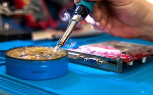
Several important stages of PCB fabrication involve chemical processing. Understanding these processes makes it easier to understand the purpose of different PCB chemicals.
Photoresist Application and Development
Photolithography is used to transfer the desired circuit pattern onto a PCB. A photosensitive material called photoresist is applied to the copper surface. Depending on the manufacturing process, the resist may be supplied as a dry film or liquid photoresist.
The board is exposed to ultraviolet light through an imaging system or phototool. The exposed or unexposed areas are then selectively removed during development, depending on whether a positive or negative resist system is being used.
The quality of the photoresist, developer concentration, exposure conditions, temperature, and development time can all affect the accuracy of the resulting circuit pattern.
Copper Etching
Etching removes unwanted copper from selected areas of the PCB to create the required conductive traces.
Common industrial etchants include cupric chloride, ferric chloride, and alkaline etching systems. Ammonium persulfate can also be used in certain applications, particularly in laboratory or prototype environments.
In production, etching chemistry must be carefully controlled because excessive etching can reduce conductor width, while insufficient etching can leave unwanted copper residues.
Factors such as chemical concentration, temperature, spray pressure, etch rate, and copper loading can affect the final result.
Electroless and Electrolytic Plating
Plating is particularly important for multilayer and double-sided PCBs because it creates conductive connections between different copper layers.
After drilling, the hole walls generally require surface preparation and an electroless copper process to establish an initial conductive layer. Electrolytic copper plating can then build up the required copper thickness.
Typical plating chemistry may include copper sulfate, sulfuric acid, chloride ions, and proprietary organic additives. Process control is essential because variations in plating chemistry can affect deposit thickness, uniformity, adhesion, ductility, and via reliability.
Solder Mask Processing
The PCB Solder Mask protects selected copper areas from environmental contamination and helps prevent unintended solder bridges during assembly.
Liquid photoimageable solder mask is widely used in modern PCB fabrication. The process generally involves coating, drying or pre-curing, imaging, development, and final curing.
The chemistry and processing conditions must be controlled to achieve accurate openings over pads and reliable adhesion to the PCB surface.
Final Cleaning
Cleaning is performed at various stages of PCB fabrication and assembly to remove contaminants such as:
- Flux residues
- Oils and fingerprints
- Dust and particles
- Processing residues
- Ionic contamination
Depending on the process, manufacturers may use deionized water, aqueous cleaners, or specialized cleaning agents.
Effective cleaning is particularly important for high-reliability electronics because ionic residues can contribute to leakage currents, electrochemical migration, and corrosion when moisture is present.
Surface Finishing
A PCB surface finish protects exposed copper pads and provides a suitable surface for component soldering.
Common finishes include:
- HASL
- Lead-free HASL
- ENIG
- ENEPIG
- OSP
- Immersion tin
- Immersion silver
Each finish uses a different chemical process and offers different combinations of solderability, shelf life, cost, flatness, corrosion resistance, and compatibility with assembly requirements.
It is important to distinguish PCB Surface Finish from solder mask. Surface finish is applied to exposed conductive pads, while solder mask is an insulating protective coating applied over areas that generally should not be soldered.
What Types of Chemicals Are Used in PCB Manufacturing?
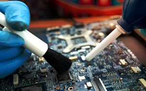
Different PCB manufacturing stages require different chemical systems. Important process parameters typically include chemical concentration, temperature, processing time, pH, solution loading, and replenishment rate.
Etching Chemicals
Etchants selectively remove unwanted copper from the PCB.
Common systems include:
- Ferric chloride
- Cupric chloride
- Alkaline copper etchants
- Ammonium persulfate for certain applications
Cupric chloride and alkaline etching systems are commonly used in industrial PCB production because their process conditions can be monitored and controlled for high-volume manufacturing.
The appropriate etchant depends on the PCB process, line configuration, copper thickness, feature geometry, and required production volume.
Photoresist Developers
Photoresist developers remove the soluble portions of photoresist after imaging.
For many PCB processes, alkaline developers based on carbonate or related alkaline chemistry are used. The exact developer depends on the type of photoresist and manufacturer’s process specifications.
Development conditions must be carefully controlled. Over-development can remove too much resist, while under-development can leave unwanted resist residues and compromise circuit definition.
Copper Plating Chemicals
Copper plating chemistry is essential for building conductive layers on PCB surfaces and inside plated-through holes.
A typical acidic copper plating system may contain:
- Copper sulfate
- Sulfuric acid
- Chloride ions
- Organic additives
The additives influence properties such as deposit uniformity, leveling, throwing power, and surface appearance.
For advanced PCB Manufacturing, plating control becomes increasingly important as manufacturers work with smaller vias, higher aspect ratios, finer traces, and more demanding reliability requirements.
Solder Mask Chemicals
Solder mask materials are generally polymer-based photoimageable or thermal-cure systems. They provide electrical insulation and environmental protection while leaving solderable pads exposed.
The processing chemistry varies according to the solder mask material and application method. Manufacturers must control coating thickness, exposure, development, curing, and adhesion to achieve reliable results.
PCB Cleaning Chemicals and Flux Removers
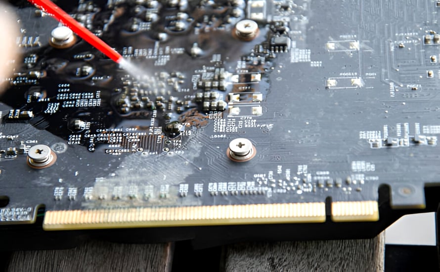
Cleaning chemicals remove residues generated during fabrication and assembly.
Depending on the application, cleaning may involve:
- Aqueous cleaners
- Mild alkaline cleaners
- Solvent-based cleaners
- Specialized flux removers
- Deionized-water rinsing
The appropriate cleaner depends on the contaminant, PCB material, component construction, assembly process, and cleanliness specification.
Surface-Finish Chemicals
Surface-finishing chemistry is used to protect exposed copper and improve solderability.
For example, ENIG uses an electroless nickel layer followed by an immersion gold layer. OSP uses an organic protective coating over exposed copper. HASL involves applying molten solder to exposed copper pads and removing excess solder to produce the required coating.
Because these processes are chemically different, manufacturers must select and control the chemistry according to the required PCB performance and assembly process.
Why Are PCB Chemicals Important in PCB Manufacturing?
PCB chemicals directly influence several aspects of PCB fabrication and assembly.
Enabling Fine and High-Density Circuitry
Modern PCB Design increasingly requires narrow traces, small pads, fine-pitch components, microvias, and tightly controlled geometries.
Accurate imaging, development, etching, and plating chemistry helps manufacturers reproduce these features consistently.
As circuit density increases, even relatively small process variations can affect conductor dimensions, insulation spacing, via quality, and overall reliability.
Preparing PCB Surfaces for Assembly
Surface preparation is essential before component assembly.
A properly processed surface finish can provide suitable solderability and protect exposed copper during storage and handling. Poor surface preparation, contamination, or inappropriate finish selection may contribute to soldering defects.
Therefore, chemical processing and PCB Assembly requirements should be considered together rather than treated as completely separate stages.
Improving Solderability and Corrosion Resistance
Appropriate surface finishes protect exposed copper from oxidation and provide a suitable interface for soldering.
This can improve assembly consistency and reduce the risk of solderability-related problems during production.
Supporting Long-Term Reliability
Chemical processes also affect the long-term reliability of a PCB.
Poor cleaning may leave ionic contamination. Inadequate plating may weaken plated-through holes or vias. Improper etching may change conductor geometry. Poor surface treatment may reduce solderability.
For high-reliability applications, chemical process control therefore forms an important part of the overall quality system.
How Should PCB Chemicals Be Handled?
Although PCB chemicals are essential to manufacturing, many process chemicals can present chemical, environmental, or occupational hazards if they are improperly handled.
Manufacturers should establish documented procedures based on the specific chemical, process, concentration, and applicable local regulations.
Understand the Chemical and Its Hazards
Before using a chemical, personnel should review its Safety Data Sheet (SDS), rather than relying solely on general assumptions about the material.
The SDS typically provides information about:
- Chemical hazards
- Required personal protective equipment
- Safe handling and storage
- First-aid measures
- Fire-fighting measures
- Spill response
- Disposal considerations
- Exposure controls
Different chemicals can have very different hazards, even when they are used for similar PCB processes.
Use Appropriate Personal Protective Equipment
Personnel handling PCB chemicals should use PPE specified by the applicable SDS and workplace risk assessment.
Depending on the chemical and operation, this may include:
- Chemical-resistant gloves
- Safety goggles or face protection
- Protective clothing or aprons
- Appropriate respiratory protection where required
PPE should be regarded as one part of a broader safety program that also includes engineering controls, ventilation, training, and safe operating procedures.
Provide Proper Ventilation and Process Controls
Some PCB chemical processes can generate vapors, aerosols, or other airborne contaminants.
Appropriate local exhaust ventilation and process enclosure can help control worker exposure. Chemical handling areas should also have suitable emergency equipment and clearly documented spill-response procedures.
Store Chemicals Correctly
Chemical storage conditions should follow the manufacturer’s SDS and applicable regulations.
Incompatible chemicals should be segregated, containers should remain properly labeled, and storage areas should be inspected regularly.
Temperature, humidity, sunlight, and other environmental conditions may affect the stability of certain chemical products, so storage requirements should be followed carefully.
Manage Waste and Chemical Disposal
PCB manufacturing generates chemical waste and process residues that must be managed responsibly.
Waste streams should be identified, segregated, labeled, stored, treated, and disposed of according to applicable environmental regulations. Chemical solutions should not simply be discharged without appropriate treatment and authorization.
PCB Chemicals and PCB Manufacturing Quality Control
Chemical management should not be viewed as an isolated activity. It is closely connected with the broader PCB Manufacturing Process.
Manufacturers can monitor parameters such as:
- Chemical concentration
- pH
- Temperature
- Processing time
- Copper loading
- Plating thickness
- Etch rate
- Surface cleanliness
- Ionic contamination
- Bath age and replenishment
Consistent monitoring helps reduce process variation and improves production stability.
For demanding applications, chemical process control should also be supported by inspection and testing, including dimensional inspection, electrical testing, surface inspection, and appropriate reliability testing.
How PCB Design Affects Chemical Processing
Although chemicals are primarily associated with fabrication rather than design, PCB Design decisions can strongly influence manufacturing requirements.
For example, trace width, spacing, copper thickness, via dimensions, hole aspect ratio, surface finish, and solder mask openings all affect how a board must be fabricated.
Designers should therefore consider manufacturability early in the design process.
A good Design for Manufacturing (DFM) review can identify features that may be difficult or expensive to manufacture before the design reaches production.
The exact design rules depend on the manufacturer’s equipment and process capabilities, so engineers should always confirm critical limits with the selected PCB fabricator.
Best Practices for Managing PCB Chemicals
A reliable chemical-management program should combine process control, worker safety, environmental management, and quality assurance.
Key practices include:
- Maintain an up-to-date inventory of process chemicals.
- Keep SDS documentation accessible to relevant personnel.
- Train employees before they work with hazardous chemicals.
- Use appropriate PPE and engineering controls.
- Monitor chemical concentration, pH, temperature, and process time.
- Establish procedures for spills and accidental exposure.
- Store incompatible chemicals separately.
- Maintain clear labeling and traceability.
- Monitor PCB cleanliness and surface quality.
- Manage chemical waste according to applicable regulations.
- Review chemical processes regularly as PCB designs and materials evolve.
- Work with qualified chemical suppliers and PCB manufacturing partners.
Conclusion
PCB chemicals are an essential part of modern printed circuit board production. They support many critical operations, including photoresist processing, copper etching, plating, solder mask processing, cleaning, and surface finishing.
Their influence extends beyond manufacturing efficiency. Properly controlled chemical processes contribute to accurate circuit geometries, reliable interconnections, good solderability, corrosion resistance, and long-term PCB reliability.
At the same time, chemical handling requires appropriate safety controls, employee training, ventilation, storage procedures, PPE, waste management, and process monitoring. For manufacturers, the goal is not simply to use the correct chemical, but to control the entire process consistently.
For engineers, understanding the relationship between PCB Design, chemical processing, PCB Manufacturing, and PCB Assembly can help create designs that are easier to manufacture and more reliable in the field. Kingda can work with customers to evaluate PCB fabrication and assembly requirements and support the transition from PCB design to production.