Zero PCB vs General-Purpose PCB: PCB Design, PCB Manufacturing & Prototyping Guide
Choosing the right prototyping board is an important step when developing an electronic prototype. Zero PCB and General-Purpose PCB are two commonly used options for building and testing circuits before moving to a custom printed circuit board.
Although these prototype boards may look similar, their copper patterns, connection methods, flexibility, and intended applications can differ. Understanding the difference between a Zero PCB and a General-Purpose PCB can help students, engineers, hobbyists, and product developers select an appropriate platform for circuit development.
This guide explains what Zero PCB and General-Purpose PCB are, how they differ, their advantages and limitations, typical applications, and when a prototype should transition to professional PCB Manufacturing.
What Is a Zero PCB?
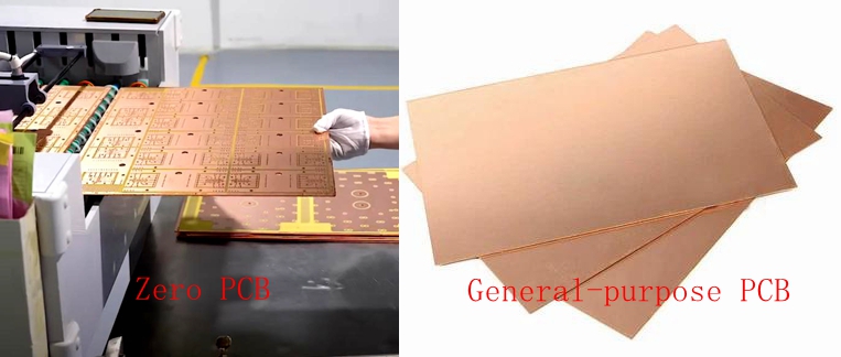
A Zero PCB is a type of universal prototyping board featuring an array of electrically isolated plated or unplated holes with individual copper pads. A common hole spacing is 2.54 mm (0.1 inch), making many versions compatible with conventional through-hole components.
Unlike a conventional fabricated PCB, a typical Zero PCB does not have predefined conductive traces connecting the pads. Instead, users create the required electrical connections manually using solder bridges, hookup wire, or jumper wires.
The term “Zero PCB” is generally used to describe a prototyping board with no predefined circuit routing. This provides considerable freedom because the user determines how each component is interconnected.
For simple circuits, this approach allows designers to quickly build and modify a circuit without first creating a complete custom PCB layout.
What Is a General-Purpose PCB?
A General-Purpose PCB, also called a general-purpose prototyping board, is a reusable or semi-standardized PCB platform designed for building, testing, and modifying electronic circuits.
The term “General-Purpose PCB” can describe several types of prototype boards depending on the manufacturer. Some have individually isolated pads, while others feature predefined copper patterns, connected rows, or other standardized layouts.
Many general-purpose boards use a 2.54 mm (0.1 inch) pitch to accommodate common through-hole components such as:
- Resistors
- Capacitors
- Diodes
- LEDs
- Transistors
- DIP ICs
- Pin headers
- Terminal blocks
Because the term can cover multiple board configurations, users should always check the actual hole pattern, copper layout, material, dimensions, and electrical specifications before purchasing a prototype board.
Zero PCB vs General-Purpose PCB: Key Differences
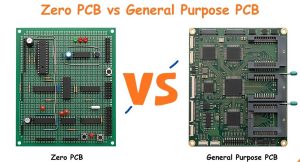
Both Zero PCB and General-Purpose PCB can be used for electronic prototyping, but the main difference is usually the copper pattern and degree of predefined connectivity.
| Comparison | Zero PCB | General-Purpose PCB |
|---|---|---|
| Definition | Prototype board with individually isolated pads and no predefined circuit routing | General-purpose prototyping board available in various standardized layouts |
| Copper Pattern | Typically isolated copper pads | May use isolated pads, connected rows, or another predefined pattern |
| Typical Pitch | Often 2.54 mm (0.1 inch) | Often 2.54 mm (0.1 inch), depending on the board |
| Circuit Flexibility | Very high because connections are created manually | Depends on the specific copper pattern |
| Assembly | Usually manual soldering and jumper wiring | Usually manual soldering; method depends on the board pattern |
| Modification | Easy to modify and rewire | Easy to modify, although predefined copper connections may affect routing |
| Mechanical Reliability | Generally more robust than a temporary breadboard once components are soldered | Similar advantages for soldered prototypes |
| Cost | Low-cost prototyping option | Generally an economical prototyping option |
| Typical Applications | DIY electronics, Arduino projects, robotics, circuit experiments | General prototyping, education, repair, laboratory projects |
| Production Use | Primarily for prototyping | Primarily for prototyping |
The most important point is that “General-Purpose PCB” is a broad category, while a Zero PCB generally emphasizes individually isolated pads and user-defined wiring.
Features of Zero PCB
A typical Zero PCB may provide the following characteristics:
- 2.54 mm (0.1 inch) hole spacing for compatibility with many through-hole components
- Individually isolated copper pads
- No predefined circuit traces
- High flexibility for custom wiring
- Compatibility with manual soldering
- Availability in different board sizes
- Single-sided or double-sided configurations, depending on the product
- FR-2 or FR-4 substrate options, depending on the manufacturer
The absence of predefined traces is one of its most important characteristics. Users can create their own connections based on the schematic rather than being restricted by an existing copper pattern.
Features of General-Purpose PCB
A General-Purpose PCB can provide a flexible platform for developing and modifying electronic circuits.
Common characteristics include:
- Standardized hole spacing on many versions
- Compatibility with common through-hole components
- Multiple board sizes and layouts
- Different substrate materials
- Easy manual component replacement
- Easy circuit modification during prototyping
- Availability with isolated pads or predefined copper patterns
Because General-Purpose PCB is a broad term, its actual features depend heavily on the specific board design.
Advantages and Disadvantages of Zero PCB
Advantages
High Design Flexibility
Because the pads are electrically isolated, users can create almost any connection arrangement required by a simple prototype.
Low Prototyping Cost
A Zero PCB can be an inexpensive way to test a circuit before investing in custom PCB Manufacturing.
Easy Circuit Modification
Components and jumper wires can be removed, replaced, or rerouted during the development process.
Useful for Learning
Zero PCB is suitable for learning soldering, component identification, basic circuit assembly, and practical electronics.
Disadvantages
Labor-Intensive Assembly
Connections must generally be created manually, which can become time-consuming as circuit complexity increases.
Difficult Routing for Complex Circuits
Large numbers of jumper wires and solder bridges can make a complicated prototype difficult to understand, troubleshoot, and maintain.
Limited Production Suitability
A manually assembled prototype board does not provide the repeatability, density, automated assembly capability, or manufacturing consistency normally required for a production PCB.
Advantages and Disadvantages of General-Purpose PCB
Advantages
- Suitable for a wide variety of electronic prototypes
- Relatively inexpensive
- Easy to modify and repair
- Available in different sizes and patterns
- Useful for education and laboratory experimentation
- Compatible with many conventional through-hole components
- Allows engineers to test hardware before custom PCB fabrication
Disadvantages
- Manual assembly can be time-consuming
- Predefined copper patterns may restrict certain circuit configurations
- Large or complex circuits can become difficult to route
- Not intended to replace a professionally manufactured production PCB
- Mechanical and electrical performance may not match a custom-designed PCB
Applications of Zero PCB
Zero PCBs are commonly used when designers need a flexible platform for quickly creating and testing circuits without manufacturing a custom board.
Arduino Projects
Zero PCB can be used to develop custom Arduino accessories such as:
- Sensor interfaces
- Motor-control circuits
- Relay circuits
- GPIO expansion boards
- Small interface circuits
This allows developers to test hardware concepts before committing to a custom PCB.
Raspberry Pi Projects
Engineers and hobbyists can use Zero PCB to create hardware interfaces for Raspberry Pi systems, including sensor interfaces, relay circuits, GPIO expansion circuits, and other accessories.
DIY Electronics
Zero PCB is useful for building small electronic projects such as:
- LED controllers
- Audio circuits
- Timers
- Simple power circuits
- Home automation prototypes
Its low cost and flexible wiring make it attractive for hobby projects.
Robotics
Robotics developers can use Zero PCB for prototyping:
- Motor-control circuits
- Sensor interfaces
- Communication circuits
- Power distribution
- Microcontroller interfaces
The prototype can be modified quickly while the overall robot hardware is still under development.
STEM and Electronics Education
Educational institutions and electronics training laboratories can use Zero PCB to teach:
- Soldering
- Component identification
- Circuit assembly
- Basic electronics
- Circuit troubleshooting
Students can gain practical experience by constructing and testing real circuits.
Product Prototyping
Engineers can use Zero PCB to verify circuit concepts, test component arrangements, and identify hardware problems before creating a custom PCB layout.
Circuit Repair and Modification
A prototype board can also be useful for temporary circuit modifications, experimental repairs, and hardware changes when a custom replacement PCB is not immediately available.
Applications of General-Purpose PCB
General-Purpose PCBs are similarly useful for building, testing, and modifying electronic circuits before moving to a custom PCB.
Electronic Prototyping
Engineers can assemble circuits on a General-Purpose PCB to evaluate functionality, test components, and identify potential design problems.
Circuit Repair and Maintenance
Technicians can use suitable general-purpose boards for experimental repairs, circuit modifications, or temporary hardware configurations.
Educational Projects
General-Purpose PCBs are widely suited to practical electronics education because students can assemble circuits and develop hands-on soldering and troubleshooting skills.
DIY Electronics
Hobbyists can use general-purpose boards for LED circuits, audio amplifiers, timers, power circuits, and home automation projects.
Product Development
During early-stage product development, engineers can use a general-purpose prototype board to validate hardware concepts before creating the final PCB Design.
Laboratory Testing
Research and development laboratories can use general-purpose boards for testing components, evaluating circuit concepts, and experimenting with hardware configurations.
Zero PCB vs General-Purpose PCB: Which Should You Choose?
The appropriate choice depends on the circuit, component type, desired flexibility, and development stage.
For Students and Beginners
A Zero PCB can provide a straightforward environment for learning soldering and basic circuit assembly because users control the connections manually.
A General-Purpose PCB can also be appropriate when its predefined copper pattern matches the circuit being developed.
For DIY Electronics Projects
Both options can work well for simple DIY projects. The decision mainly depends on whether you want completely custom wiring or prefer a board with a predefined pattern.
For Arduino and Raspberry Pi Projects
Both types can be used for prototyping sensor interfaces, expansion circuits, motor-control circuits, communication modules, and other hardware accessories.
For Engineers and Product Developers
Either board can be useful during early prototyping. However, as the circuit becomes more complex, a custom PCB provides greater control over routing, component placement, electrical performance, mechanical dimensions, and manufacturing repeatability.
For Production-Ready Products
Once the circuit has been validated, the design should generally transition from a manually assembled prototype to a professionally designed and manufactured PCB.
At this stage, engineers can optimize the PCB Design for manufacturability, assembly, thermal management, signal integrity, and reliability before beginning full-scale PCB Manufacturing.
Common Mistakes When Choosing a Prototype PCB
Selecting the right prototype board is important for efficient circuit development. Beginners commonly make several mistakes.
Choosing a Board Without Considering Circuit Complexity
A small prototype board may be sufficient for a simple circuit but become difficult to use when the number of components and connections increases.
Using a Prototype Board as a Production PCB
Prototype boards are useful for development and testing, but they generally lack the optimized routing, repeatability, automated assembly compatibility, and manufacturing controls required for production products.
Ignoring PCB Material
Different substrate materials provide different mechanical and thermal characteristics. FR-2 may be suitable for some low-cost applications, while FR-4 is commonly used where greater mechanical and thermal performance is required.
The correct material should be selected according to the application’s electrical, mechanical, thermal, and environmental requirements.
Choosing the Wrong Board Size
A board that is too small can make component placement and wiring difficult, while an unnecessarily large board can increase material usage and make the prototype less representative of the final product.
Failing to Plan the Transition to Custom PCB Manufacturing
A successful prototype should eventually be converted into a manufacturable PCB design. Engineers should consider component footprints, routing, board dimensions, stackup, manufacturing tolerances, assembly requirements, and testing requirements before moving to production.
How to Transition From a Prototype to a Custom PCB
Once the circuit has been successfully validated on a Zero PCB or General-Purpose PCB, the next stage is to create a professional PCB layout.
A typical transition process includes:
- Finalize the schematic.
- Select production-ready components.
- Verify component footprints.
- Create the PCB outline.
- Define the layer stackup.
- Place components according to electrical and mechanical requirements.
- Route power and signal traces.
- Add ground planes and thermal structures where necessary.
- Run design-rule checks.
- Perform DFM and DFA reviews.
- Generate fabrication and assembly documentation.
- Manufacture and assemble a prototype PCB.
- Test and revise the design before production.
This process transforms a manually wired prototype into a repeatable PCB Manufacturing Process.
Conclusion
Zero PCB and General-Purpose PCB are both useful tools for electronic prototyping, especially when engineers, students, or hobbyists need to build and modify circuits without immediately producing a custom PCB.
The key distinction is the copper pattern. A typical Zero PCB provides individually isolated pads with no predefined circuit routing, giving users extensive freedom to create their own connections. A General-Purpose PCB is a broader category that may include isolated pads or predefined copper patterns.
Neither type is intended to replace a professionally manufactured PCB for most production applications. Instead, they serve as practical development platforms for validating circuit concepts, testing components, learning electronics, and identifying design problems.
After the prototype has been validated, moving to a professional PCB Design and PCB Manufacturing workflow allows engineers to achieve more controlled routing, optimized component placement, better mechanical integration, improved manufacturing consistency, and greater production reliability.