Application Processor Board Design: Interfaces and Layout Demands
An application processor is a system on a chip that expects to be surrounded by memory, storage, display, camera and network interfaces, and a board designed around one is judged by how well it delivers those interfaces rather than by the processor itself. The layout challenge is concentrated in a small area: a fine-pitch device with a wide memory bus, several high-speed serial links and a dozen supply rails, all of which have to be routed without interfering with each other.
What the Device Expects Around It
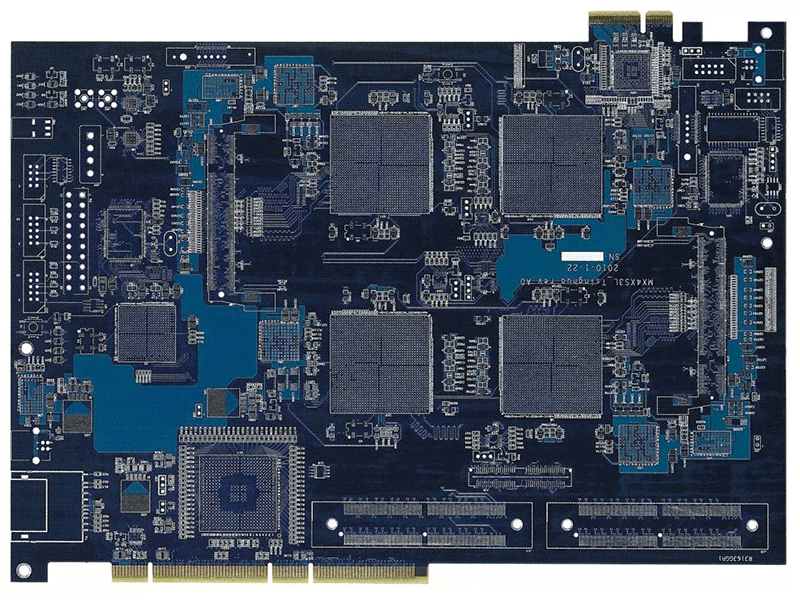
A modern application processor integrates a heterogeneous cluster of high-performance and high-efficiency cores, a graphics processor, video encode and decode engines, an image signal processor and a set of high-speed interfaces. The integration reduces the component count but concentrates the electrical demands: the display and camera links, the memory bus and the power delivery network all converge on one package.
This convergence is what sets the layer count. Escape routing from a fine-pitch package often consumes a layer pair on its own, and the remaining interfaces have to be distributed across the rest without violating their reference requirements.
Memory Bus and Bandwidth
The memory interface is usually the widest and fastest bus on the board. It should be routed with a continuous reference plane beneath it, with the byte lanes length-matched within each group and the groups matched to each other within the tolerance specified by the device. Routing on a single layer is preferable, because every via introduces a discontinuity, and the number of layers required is often determined by whether the bus can be kept on one.
Where the device supports dual rank or a wide data bus, the routing area grows quickly. The practical approach is to place the memory devices so that the bus runs in a straight corridor from the processor to the memory, and to reserve that corridor in the stack-up before any other interface is routed.
High-Speed Serial Links
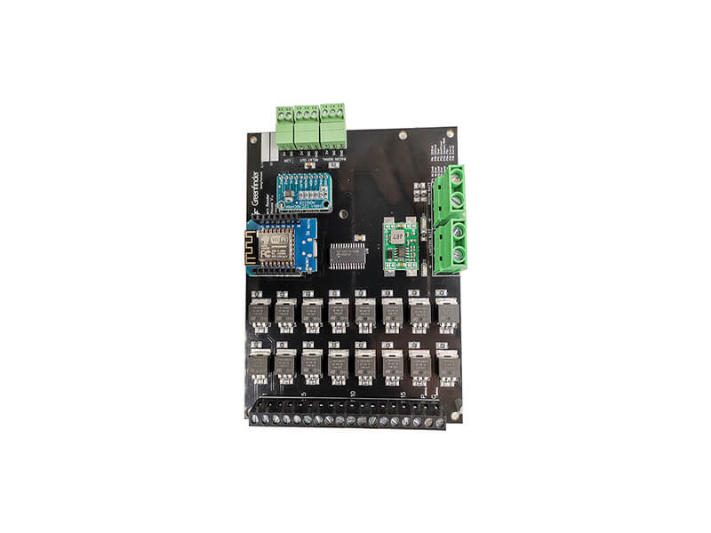
Camera, display, storage and expansion interfaces all use high-speed serial links, and each has its own requirement. The camera interface is typically a MIPI arrangement of differential lanes that must be length-matched as a group and kept away from switching supplies. The display interface may be the same arrangement or an embedded display interface with its own lane count. Storage and expansion are commonly routed as PCI Express lanes, which require controlled impedance, tight intra-pair matching and a reference plane that is not split beneath them.
All of these links share one property: they launch from the processor on adjacent pins and they need separate corridors. Planning those corridors is the principal placement task on the board. Our layer assignment guidance describes how to reserve them in the stack-up.
Power Delivery and Sequencing
An application processor typically requires a core rail, a graphics or system rail, a memory rail and several auxiliary rails, each with its own regulation and its own sequence. Power integrity is determined less by the choice of regulators than by the impedance of the network that carries the current from them to the device, and that impedance is a function of the plane structure and the placement of the decoupling capacitors.
The decoupling strategy follows the usual progression: a large capacitance somewhere near the rail, mid-value capacitors distributed along the load, and a small capacitor at each supply pin. Placing the smallest capacitors at the pins is what keeps the loop area low at the frequencies where the device draws its switching current. Where the processor has a large number of supply pins in a ball grid array, the capacitors are inevitably on the opposite side of the board, tied through vias, which makes the via arrangement part of the decoupling design.
Thermal Considerations
An application processor under sustained load dissipates enough heat to require a deliberate path to the ambient or to a metal part. The device package usually has a thermal pad, and the board underneath it should have a matching copper area with thermal vias to the opposite side. Where the product has a metal housing, a gap filler or a thermal pad between the package and the housing is far more effective than the board alone.
The thermal design also constrains the placement of the processor. Putting it in a corner of the board halves the area available to spread heat, while placing it centrally allows copper to conduct in all directions. Our thermal management notes cover the conduction path.
Bring-Up and the Development Board Case
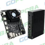
A development board adds requirements that a product board does not have: a boot medium that can be changed, a debug header, expansion connectors and often a power monitoring facility. Each of those adds a connector, a signal path and a mechanical constraint, and the debugging interfaces in particular have to be routed so that they can be probed without disturbing the high-speed links.
The most common development board problem is not an electrical one. It is that the boot configuration is inaccessible, or that a rail cannot be measured because the test point is on the opposite side of the board from the regulator. Providing test points on the rails and a clearly marked boot configuration facility costs almost nothing at design time and saves hours during bring-up. The design release checklist covers the bring-up provisions, and the component tolerance and reliability material covers the derating decisions that apply to a board running at high current.
Configuration and Boot Facilities
Most processors select their boot source from a set of strapping pins sampled at reset, and those pins are usually shared with functional signals. Whether the straps are implemented with resistors that can be moved, with a switch, or with a connector gives different amounts of flexibility during development. Placing the strapping resistors where they can be changed without removing the processor from its socket, and documenting the combinations, prevents the most common cause of a board that does not start.
Where the boot medium is removable, the interface to it should be placed so that inserting and removing a card does not obstruct the debug header. These are mechanical details, but a development board that cannot be debugged conveniently costs more time than any electrical refinement it might gain.
FAQ
How many layers does an application processor board need? Six to ten layers is the usual range. The lower end applies where the memory bus can be routed on one layer and the serial links have generous corridors, and the upper end where the bus is wide, several high-speed interfaces are present and the escape routing from the package is dense. The count should be decided after the interface corridors have been identified, not before.
Is the memory bus or the serial link routing more difficult? The memory bus is harder to place because it is wide and needs a continuous corridor, while the serial links are harder to route precisely because they demand controlled impedance and tight length matching. The bus usually determines the stack-up, and the serial links determine how much of the remaining routing area can be used for anything else.
What does gopcb need to review such a design? We need the stack-up, the interface list with the reference requirements for each, and the power distribution plan. Because these three are interdependent on a processor board, reviewing them together before the layout is finalised is the most effective way to avoid a design that satisfies every interface individually but cannot be manufactured as drawn.