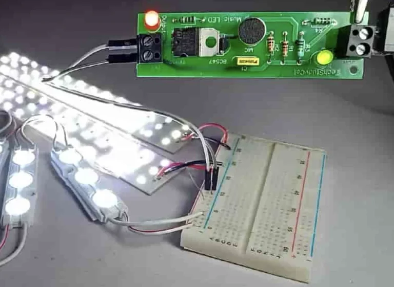
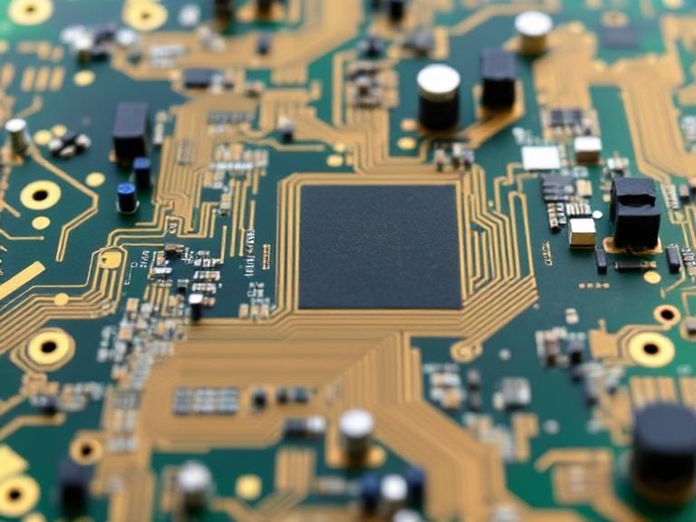
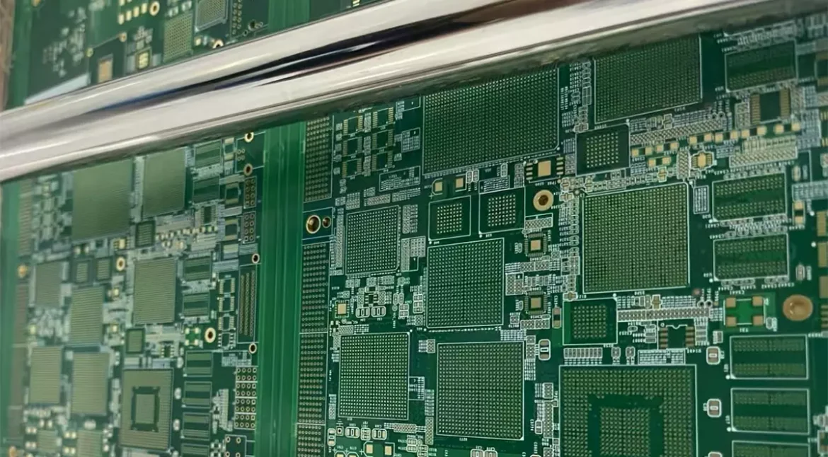
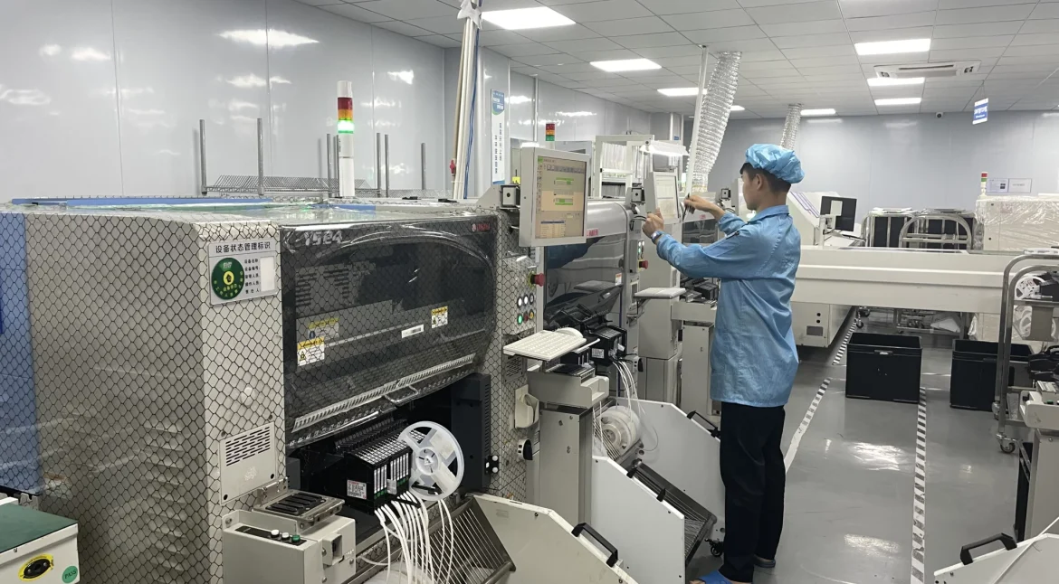
Motion Sensor PCB Price: PIR, Microwave and Integrated A motion sensor board sits at the boundary between analogue and digital design. The sensor produces a very small, very slow signal, the processor beside it runs at tens of megahertz, and the power supply switches at hundreds of kilohertz on the…
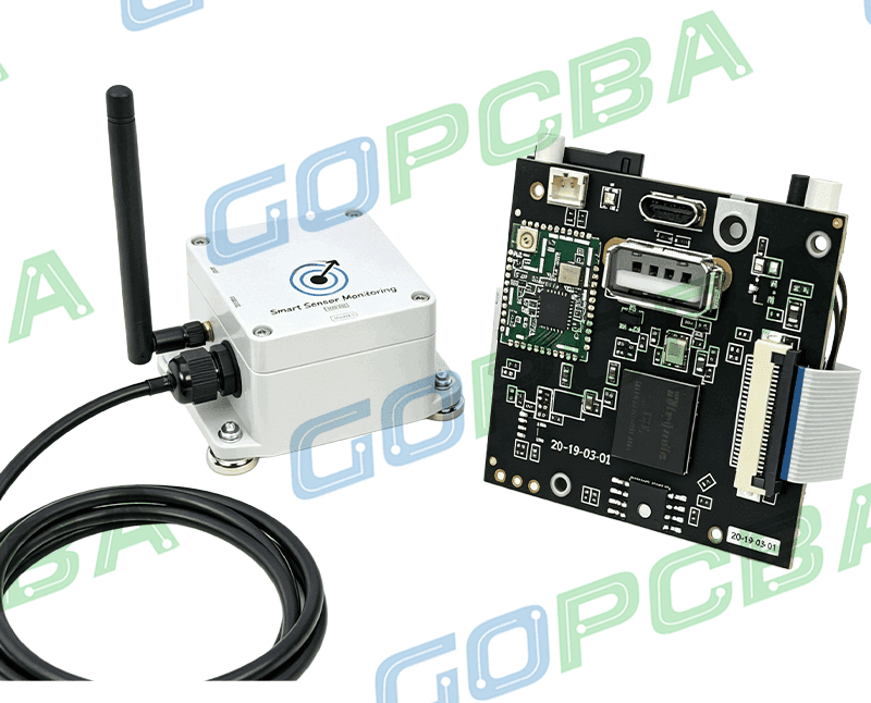
PCB Antenna Layout Considerations for Wireless Designs A radio performs only as well as the copper that feeds it. Antenna layout decides how efficiently power leaves the board, how much of it returns as unwanted coupling, and whether the product passes certification on the first attempt. The rules are not…
Practical Notes on Backdrilling A plated through hole is convenient, but the unused portion of the barrel below the last layer it serves is not electrically neutral. That leftover copper acts as a stub, and at high frequencies it behaves as a resonant element that degrades the channel. Backdrilling removes…
Where to Place an Unavoidable Impedance Discontinuity Every high speed link contains at least one place where the impedance is not what the stackup drawing promises. It might be a connector, a package, a via that has to change layers, or a component pad that is wider than the trace.…
PCB Traceability Marking: Codes That Survive the Process Traceability on a printed circuit board is usually treated as a labelling problem, but the marking is only the visible end of a chain that begins with the material batch and ends with the shipping carton. Where that chain is broken, a…
USB Differential Pair Routing on a PCB USB is the interface most engineers meet first and one of the easiest to get subtly wrong. The pair looks like any other differential route, the data rate on the label is modest by modern standards, and the connector is often placed by…
Blind and Buried Via Design Rules: An HDI Stack-Up Guide Blind and buried vias are the reason a dense board can be routed at all. They let a signal travel between two inner layers without drilling through the whole panel, freeing the surface for components and shortening the return path…
Autorouting High Speed Digital PCBs: Why It Falls Short Autorouters have improved enormously, and for many boards they are genuinely useful. Yet on a high speed digital design they still produce results that experienced engineers reject, and the reason is not that the algorithms are weak. It is that the…
Two-Layer Board: Two-Layer vs Four-Layer PCB: What the Extra Layers Buy The number of copper layers is the single choice that most affects the cost of a board, and it is usually made early, on the strength of an estimate rather than a calculation. Understanding what the second and third…
Solder Wicking and Thermal Relief Design in PCB Layout Two solder problems that look unrelated share the same root cause. Solder wicking pulls molten alloy where it does not belong, and thermal relief design decides how heat moves between a pad and the plane it touches. Both are controlled by…