PCB Material Selection: Dielectric, Thermal and Structural Properties Every thermal, mechanical and electrical behaviour of a board is set by the material it is built from. Copper geometry gets most of the attention during layout, but the substrate decides the impedance, the loss, the dimensional stability and the temperature at…
Test Point Design: Coverage, Placement and ICT Access Test points are the interface between the board and the equipment that verifies it. They are cheap to add during layout and expensive to add afterwards, and their placement determines whether a bed of nails fixture can reach every net or whether…
PCB Layout Isolation Rules: Separating Noisy and Sensitive Circuits Most noise problems on a mixed-signal board come from two circuits that were placed too close together. The remedy is not a clever component but a set of separation rules applied consistently from the first placement decision: keep the strong away…
FPC Lamination Process: Stacking, Release Film, and Structure Lamination is the operation that turns a stack of flexible layers into a single bonded circuit, and it is the step that most distinguishes flexible board production from rigid board production. The materials are thinner, the handling requirements are stricter, and the…
PCB Placement Principles: Partitioning by Function and Signal Class Placement is the stage where the electrical intent of a circuit is translated into a physical floorplan, and it sets the ceiling on what the routing can achieve. A board with a careless placement cannot be rescued by careful routing, because…
Via Design in High-Speed PCB Layout: Parasitics and Stubs A via looks like a simple connection between two layers, and electrically it is anything but simple. Every via adds capacitance to the net it joins, adds inductance to the return path around it, and creates a stub that reflects energy…
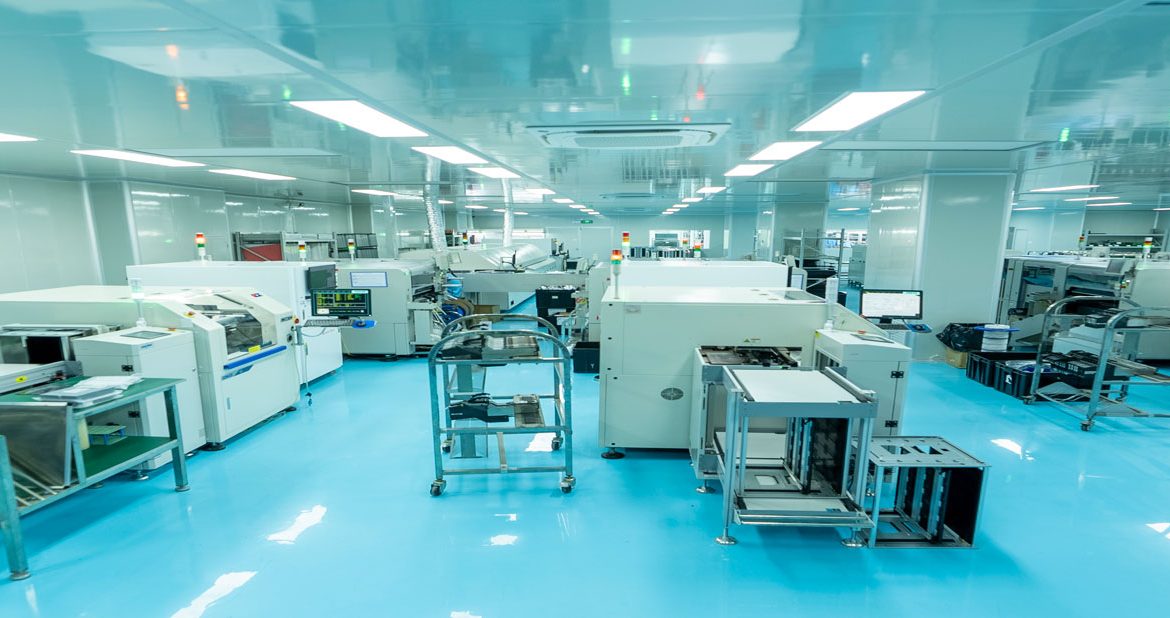
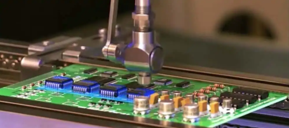
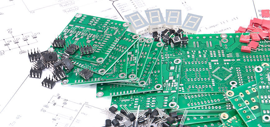
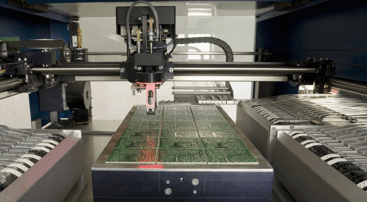
5 Key Stages of PCB Prototype Manufacturing Almost everyone who works with electronics knows what a printed circuit board is, and far fewer know how one is actually built. Modern boards are constructed with a pattern plating process, in which copper is plated onto the areas that will become conductors…
OSP Surface Finish: Process and Protection Copper oxidises. A bare copper pad that has been exposed to air for a few days will not wet properly when solder is applied, and the resulting joint is weak and unreliable. Preventing that means covering the copper until the moment of assembly, and…
Multilayer PCB Design Tolerances Explained Every dimension on a fabrication drawing carries a tolerance, and every tolerance costs money to hold. The skill in a multilayer design is not to demand the tightest value everywhere, but to identify the few dimensions where accuracy actually matters and to leave the rest…
Board Size and Cutting Dimensions for PCB Prototypes The outline of a board looks like the simplest part of a design, and it is usually the last thing anyone checks. In practice board size is constrained by the panel the fabricator runs, and the way the boards are separated from…