KingdaKingdaKingda

Call Us 24/7

+86-181-2376-9076

Send Us Mail

sales@gopcba.com

Our Location

Baoan District, Shenzhen, China

Language

  • enEnglish
    • fr France
    • itItalian
Kingda
  • Home
  • PCB Assembly
    • Prototype PCB Assembly
    • Turnkey PCB Assembly
    • Low Volume PCB Assembly
    • High Volume PCB Assembly
    • SMT PCB Assembly
    • Through-Hole PCB Assembly
    • Mixed Technology PCB Assembly
    • Flex PCB Assembly
  • Services
    • PCB Design/Layout
    • PCB Manufacturing
    • Rapid PCBA Prototyping
    • Components Procurement
    • Conformal Coating
    • PCBA Testing
    • Box Build Assembly
    • Wire & Cable Harness Assembly
  • Industry Solutions
    • Medical PCBA
    • Telecommunications PCBA
    • Energy PCBA
    • Industrial PCBA
    • Artificial Intelligence PCBA
    • IOT PCBA
  • Resources
    • PCB Capabilities
    • PCBA Capabilities
    • FAQ
    • Blog
  • About Us
    • About Us
    • Why Us
    • Quality Management
  • Contact Us
Get A Quote
218

Solder Mask Curing: Key Checks Before Release

  • By Frank guo
  • 2026年 9月 13日
  • PCB Assembly
  • No Comments
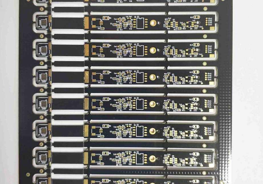
Solder Mask Curing: Key Checks Before Release Solder mask curing is the sequence of tack dry, UV exposure and thermal bake that turns a printed liquid film into a hard, chemically resistant coating. Shorten a stage and the mask can pass a visual check while still being soft and under-reacted,…
Continue Reading
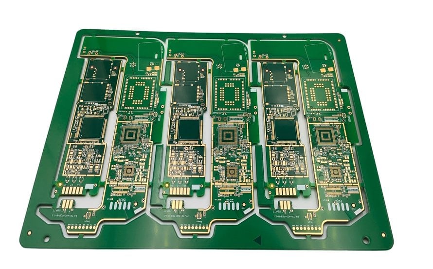
PCB manufacturing

Plating Throw: Key Checks Before Release

  • By Frank guo
  • 2026年 9月 13日
  • PCB Assembly
  • No Comments
Plating Throw: Key Checks Before Release Plating throw is the ratio of copper thickness at the centre of a hole to the thickness deposited on the surface of the same panel. A bath with good throw builds a hole wall that is nearly as thick as the surface copper, while…
Continue Reading
PCB Assembly Process

Bad Mark: Key Checks Before Release

  • By Frank guo
  • 2026年 9月 13日
  • PCB Assembly
  • No Comments
Bad Mark: Key Checks Before Release A bad mark is a signal that tells the placement machine a unit inside the panel has already failed and must be left empty. The mark is applied after the electrical test or the inspection step that found the fault, and it travels with…
Continue Reading
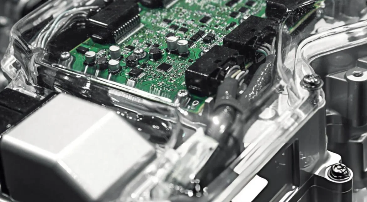
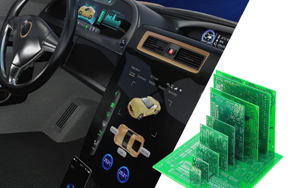
Automotive PCB

Solder Mask Curing: 6 Stages From UV Tack to Final Bake

  • By Frank guo
  • 2026年 9月 13日
  • PCB Assembly
  • No Comments
Solder Mask Curing: 6 Stages From UV Tack to Final Bake Solder mask curing is the sequence of tack dry, UV exposure and thermal bake that turns a printed liquid film into a hard, chemically resistant coating. Shorten a stage and the mask can pass a visual check while still…
Continue Reading
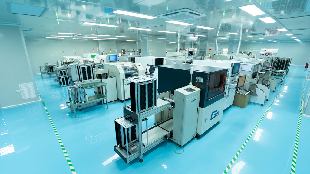
SMT车间一角

Pattern Plating on PCB: 7 Controls That Fix Copper Thickness

  • By Frank guo
  • 2026年 9月 13日
  • PCB Assembly
  • No Comments
Pattern Plating on PCB: 7 Controls That Fix Copper Thickness Pattern plating is the electrolytic step that builds copper on the traces and inside the drilled holes after the plating resist has defined which areas will be plated. It follows the electroless copper that makes the hole walls conductive, and…
Continue Reading
PCB Assembly

Pick Height on SMT Feeders: 5 Setup Rules

  • By Frank guo
  • 2026年 9月 13日
  • PCB Assembly
  • No Comments
Pick Height on SMT Feeders: 5 Setup Rules Pick height is the Z position at which the vacuum nozzle meets the component inside the tape pocket. The machine closes the vacuum at that point and waits for a pressure switch or a flow sensor to confirm that a part is…
Continue Reading
Applications_of_Automobile_PCBs

Half Ounce Copper: Where 0.5 oz Foil Fits in a Stack-Up

  • By Frank guo
  • 2026年 9月 13日
  • PCB Assembly
  • No Comments
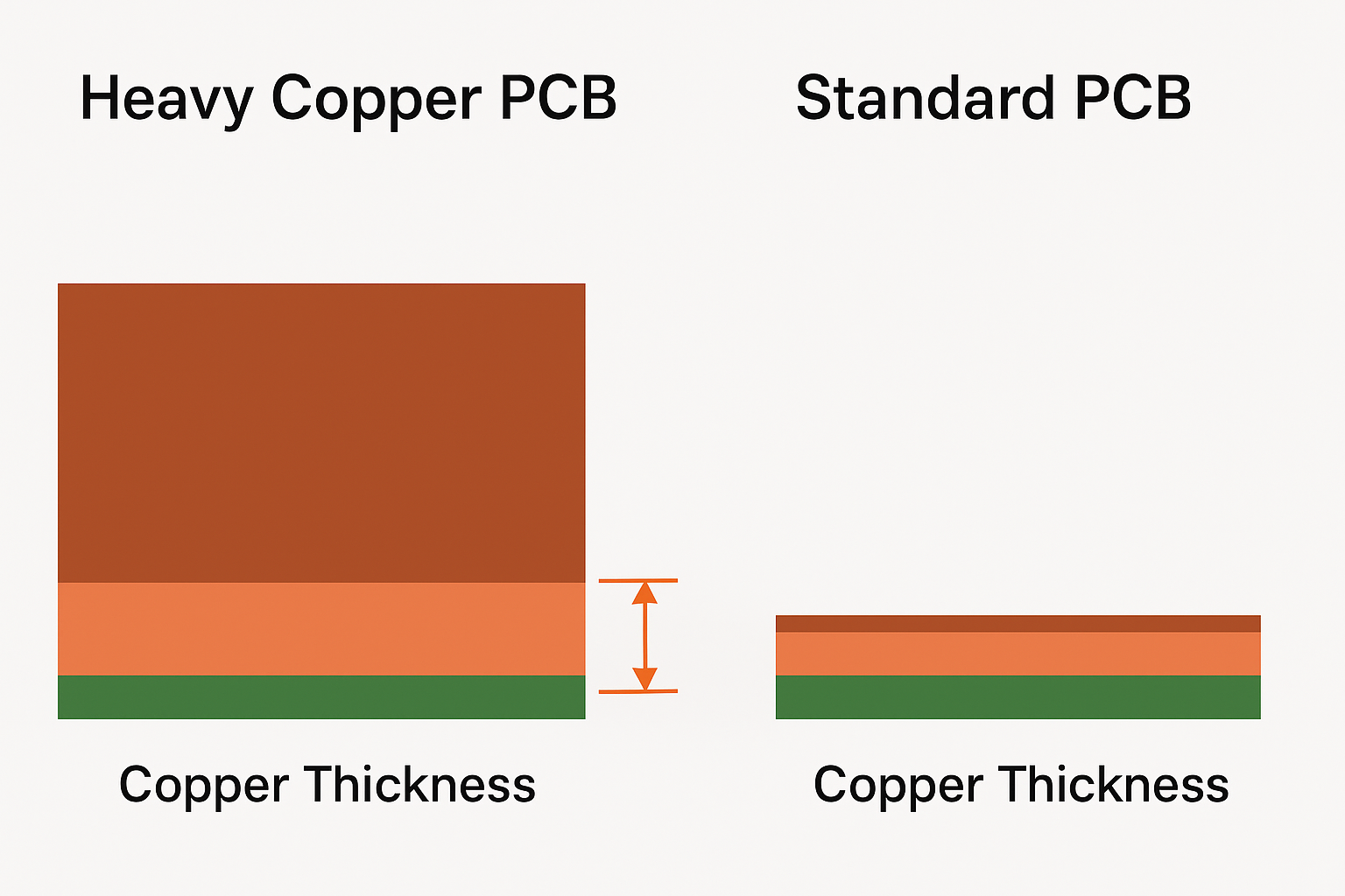
Half Ounce Copper: Where 0.5 oz Foil Fits in a Stack-Up Half ounce copper is foil rolled to about 17.5 micrometres nominal thickness, half the weight of the standard one ounce foil. It is chosen when the design needs finer traces, a thinner finished board or a lighter panel, and…
Continue Reading
HDI-PCB-design

Brown Oxide: Design Rules and Process Limits

  • By Frank guo
  • 2026年 9月 13日
  • PCB Assembly
  • No Comments
Brown Oxide: Design Rules and Process Limits Brown oxide treatment is the chemical step that grows a controlled copper oxide layer on inner layer copper so the prepreg can bond to it during lamination. The copper leaves the line with a matte, dark brown surface built from fine dendrites. That…
Continue Reading
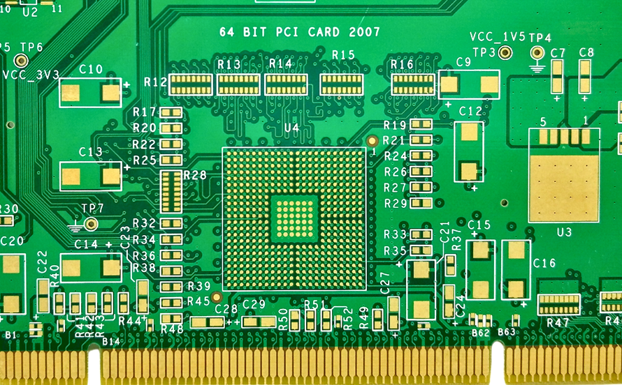
Quick-Turn-PCB-Fabrication-Viasion-1

Brown Oxide: 6 Rules for Multilayer Lamination Bonding

  • By Frank guo
  • 2026年 9月 13日
  • PCB Assembly
  • No Comments
Brown Oxide: 6 Rules for Multilayer Lamination Bonding Brown oxide is the copper oxide grown deliberately on inner layer copper before a multilayer board is pressed. Its job is not to glue the layers together; it is to give the prepreg a surface the resin can wet and grip, so…
Continue Reading
through-hole PCB assembly

Plating Throw: 7 Controls That Improve Copper in Holes

  • By Frank guo
  • 2026年 9月 13日
  • PCB Assembly
  • No Comments
Plating Throw: 7 Controls That Improve Copper in Holes Plating throw is the ratio of copper thickness at the centre of a hole to the thickness deposited on the surface of the same panel. A bath with good throw builds a hole wall that is nearly as thick as the…
Continue Reading
1 … 79 80 81 … 591

Search Posts

Categories

  • Electronic Materials
  • Electronical Engineering
  • Industrial Control
  • PCB Assembly
  • PCB Design
  • PCB Manufacturing

Recent Posts

Surface Mount Technology (SMT): Process, Components, Design Guidelines & PCB Assembly

Surface Mount Technology (SMT): Process, Components, Design Guidelines & PCB Assembly

Zane Zhang - 2026年 10月 2日
Cheap PCB Costs: PCB Design, PCB Manufacturing & SMT vs TH Guide

Cheap PCB Costs: PCB Design, PCB Manufacturing & SMT vs TH Guide

Jelly - 2026年 9月 30日
Cheap PCB Costs: PCB Design, PCB Manufacturing & SMT vs TH Guide

Cheap PCB Costs: PCB Design, PCB Manufacturing & SMT vs TH Guide

Jelly - 2026年 9月 30日

Tags

AOI inspection automotive electronics automotive PCBA quality automotive standards box build assembly component mounting component procurement component supplier conformal coating defect prevention DFM checks DFM review e-bom management electronic component shortage electronic manufacturing services electronic manufacturing standards Electronic Materials electronics design best practice electronics manufacturing capacity electronics sourcing high volume production industrial electronics insertion mount manufacturability review mass production quality mixed technology PCB PCBA inspection PCBA prototype PCBA turnkey PCBA volume pricing PCB Design PCB layout rules PCB Manufacturing PCB sourcing power electronics PCB printed circuit board prototype quick turn PCB reflow soldering SMT assembly quality SMT production solder paste inspection solder paste printing surface mount technology vehicle electronics wave soldering
GOPCBA-logo

As a professional China PCB assembly manufacturer, we provide a full range of electronic manufacturing services from PCB fabrication, PCBA to OEM/ODM, including PCB design, PCB layout, rapid PCBA prototyping, components procurement, SMT/ THT assembly, china pcb assembly, china pcb prototype, PCBA testing and box build assembly.

Linkedin Facebook-f X-twitter Youtube Instagram

PCB ASSEMBLY

  • Prototype PCB Assembly
  • Low Volume PCB Assembly
  • High Volume PCB Assembly
  • Turnkey PCB Assembly
  • SMT PCB Assembly
  • Through-Hole PCB Assembly
  • Mixed Technology PCB Assembly
  • Flex PCB Assembly

OUR SERVICES

  • PCB Design/Layout
  • PCB Manufacturing
  • Rapid PCBA Prototyping
  • Components Procurement
  • Conformal Coating
  • PCBA Testing
  • Box Build Assembly
  • Wire & Cable Harness Assembly

TECHNICAL SUPPORT

  • About Us
  • Quality Management
  • Artificial Intelligence PCBA
  • Industrial PCBA
  • IOT PCBA
  • Medical PCBA
  • Energy PCBA
  • Telecommunications PCBA

Copyright © 2026. Shenzhen Kingda Electronics Co., LTD  All rights reserved. 

  • Sitemap
  • Terms of Service
  • Privacy Policy
Zmdi Zmdi-email Phone-square Whatsapp Weixin
x

ABOUT US

Progressively maintain extensive infomediaries via extensible nich. Capitalize on low hanging fruit. a ballpark value added is activity to beta test. Override the digital divide with additional click throughs from fruit.

LOCATIONS

map

New York Office

+07 554 332 322
contact@example.com
office@example.com
37 San Fairport, NY 14450, New York City
All Locations

FOLLOW US