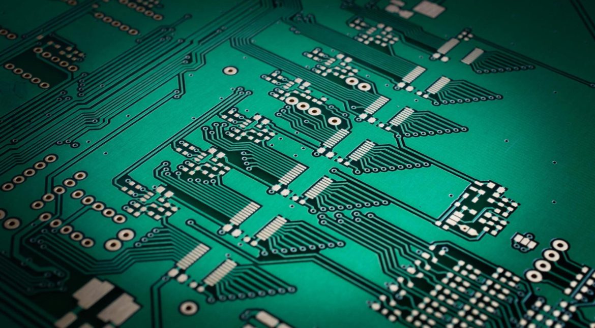
8-Layer PCB Stackup: PCB Design, PCB Manufacturing & Layer Stackup Guide
As electronic products become smaller, faster, and more functionally complex, conventional 2-layer and 4-layer circuit boards are often unable to provide sufficient routing space, signal isolation, and power distribution. This is where an 8-layer PCB becomes particularly useful.
An 8-layer printed circuit board provides additional routing layers and reference planes for complex electronic designs. Compared with 2-layer, 4-layer, or 6-layer PCBs, an 8-layer board offers more flexibility for separating high-speed signals, power distribution, and sensitive circuits while maintaining a controlled electrical environment.
A carefully engineered 8-layer PCB stackup normally includes multiple signal layers, ground planes, and power planes separated by dielectric materials such as core and prepreg. The arrangement of these layers directly affects signal integrity, impedance control, electromagnetic interference (EMI), thermal performance, manufacturability, and overall cost.
For engineers working on advanced PCB Design, understanding the physical structure and electrical behavior of an 8-layer stackup is essential. This article explains typical 8-layer PCB stackup configurations, the functions of different layers, major design considerations, advantages, applications, and important PCB Manufacturing factors.
What Is a Typical 8-Layer PCB Stackup?
A typical 8-layer PCB stackup consists of eight conductive copper layers separated by dielectric materials.
The dielectric structure generally contains:
- Prepreg
- Core materials
- Copper foil
- Copper-plated vias and holes
An 8-layer board can be configured in several different ways. A common approach is to combine four signal layers with four plane layers, although the exact arrangement depends on the application.
For example, the plane layers may be assigned to:
- Ground
- Power
- Ground
- Power
Alternatively, some designs may use more signal layers and fewer dedicated power planes.
The purpose of the stackup is not simply to increase the number of copper layers. It is to create an electrical and mechanical structure that provides suitable reference planes, controlled impedance, manageable routing density, and reliable manufacturing.
Adding more layers generally increases fabrication complexity and cost, but it can substantially reduce routing congestion and improve electrical performance when properly designed.
8-Layer PCB Stackup Structure
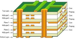
Before designing an 8-layer board, engineers should understand how the individual layers interact.
A simplified cross-section may contain:
| Layer | Typical Function |
|---|---|
| L1 | Top signal / component layer |
| L2 | Ground reference plane |
| L3 | Internal signal layer |
| L4 | Power or ground plane |
| L5 | Power or ground plane |
| L6 | Internal signal layer |
| L7 | Ground reference plane |
| L8 | Bottom signal / component layer |
This is only one example. The actual PCB layer stackup should be optimized according to routing density, signal speed, impedance requirements, power distribution, dielectric thickness, copper weight, and manufacturing capability.
The dielectric thickness between a signal layer and its reference plane is particularly important. A smaller separation can provide stronger electromagnetic coupling to the reference plane and can make controlled-impedance routing easier to achieve with practical trace widths.
Four Common 8-Layer PCB Stackup Configurations
There are many possible ways to arrange eight PCB layers. The optimal structure depends on the application, signal-speed requirements, component density, power architecture, and manufacturing process.
Four representative configurations are shown below.
| Layer | Type 1 | Type 2 | Type 3 | Type 4 |
|---|---|---|---|---|
| L1 | Signal | Ground | Signal 1 | Signal 1 |
| L2 | Ground | Signal 1 | Ground | Ground |
| L3 | Power | Power | Signal 2 | Signal 2 |
| L4 | Signal 2 | Signal 2 | Ground | Power |
| L5 | Signal 3 | Signal 3 | Power | Ground |
| L6 | Ground | Ground | Signal 3 | Signal 3 |
| L7 | Power | Signal 4 | Ground | Power |
| L8 | Signal 4 | Ground | Signal 4 | Signal 4 |
These configurations should be treated as starting points rather than universal standards.
Type 1: Signal Layers With Multiple Reference Planes
This structure provides multiple ground and power planes around the signal layers.
The ground planes provide low-impedance return paths and can help reduce electromagnetic coupling between adjacent signal layers. The arrangement can be useful for designs that require multiple signal layers while maintaining reasonable signal integrity.
However, power-plane placement must be carefully evaluated to avoid creating undesirable return-current paths.
Type 2: Ground-Plane-Rich Structure
This configuration places ground planes strategically between signal layers.
The additional ground references can improve shielding and reduce coupling between signal layers. However, routing transitions between layers may require careful via planning because signals can encounter plane boundaries or changes in their reference environment.
Designers should always consider the return-current path when routing signals between different reference planes.
Type 3: Centrally Coupled Power and Ground Planes
In this configuration, power and ground planes are positioned close to one another in the internal stackup.
A closely coupled power-ground pair can provide a low-inductance power-distribution structure and improve high-frequency power integrity.
This arrangement can be particularly useful when the board contains high-speed digital circuitry and requires a stable power-distribution network.
Type 4: Signal-Focused Configuration
This structure provides a relatively large number of signal layers while incorporating power and ground planes into the internal stackup.
It can offer substantial routing capacity, but the designer must pay close attention to reference-plane continuity, return paths, impedance control, and power distribution.
There is no universal “best” 8-layer stackup. The correct configuration depends on the electrical and mechanical requirements of the specific PCB.
Functions of Plane Layers in an 8-Layer PCB
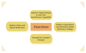
Reference planes play a critical role in an 8-layer PCB stackup.
Improving Signal Integrity
A continuous ground reference provides a predictable return-current path for high-speed signals.
When the reference plane is continuous and close to the signal layer, the electromagnetic field is more tightly contained between the trace and its reference plane. This can help reduce crosstalk and unwanted radiation.
An interrupted reference plane, however, can force return current to take a longer path, potentially increasing loop area and electromagnetic emissions.
Reducing Noise and Signal Reflection
Ground and power planes help establish controlled electrical environments for signal routing.
For high-speed designs, the relationship between trace geometry, dielectric thickness, copper thickness, and reference planes determines controlled impedance.
If a high-speed signal crosses a split or gap in its reference plane, its return path can become discontinuous, which may increase noise and signal-integrity problems.
Improving Power Integrity
Closely coupled power and ground planes can reduce power-distribution inductance and provide distributed capacitance.
This can complement local decoupling capacitors placed near integrated circuits.
However, plane capacitance should not be treated as a replacement for properly selected and strategically placed discrete decoupling capacitors.
Providing Electromagnetic Shielding
Ground planes can act as electromagnetic shields between signal regions and help reduce coupling between sensitive circuits.
For example, sensitive analog circuitry can be separated from noisy digital routing through appropriate layer assignment, grounding, physical spacing, and return-path management.
Key 8-Layer PCB Stackup Design Considerations
The layer stackup should be developed early in the PCB Design process because changing it later can affect routing, impedance, manufacturing, and mechanical dimensions.
1. Layer Assignment
An 8-layer PCB commonly uses multiple signal and plane layers.
A practical stackup may include:
- Four signal layers
- Two or three ground planes
- One or two power planes
The exact allocation should be determined from the actual routing and power-distribution requirements rather than applying a fixed formula.
2. Signal Routing
Adjacent signal layers should be considered carefully to minimize crosstalk.
Engineers can improve isolation by:
- Providing adequate spacing between traces
- Using continuous reference planes
- Alternating routing directions where appropriate
- Keeping high-speed signals away from noisy power regions
- Minimizing unnecessary parallel routing
- Maintaining consistent reference planes
For high-speed interfaces, trace geometry and reference-plane spacing should be established before detailed routing begins.
3. Reference Plane Distribution
Every high-speed signal should have a suitable reference plane.
A signal routed on an internal layer without a continuous nearby reference can experience a less predictable return-current path.
Therefore, the stackup should be evaluated not only by the number of signal layers but also by the quality and continuity of their reference planes.
4. Impedance Control
Controlled impedance is one of the most important considerations in high-speed PCB Design.
The impedance of a PCB trace depends on several factors, including:
- Trace width
- Copper thickness
- Dielectric thickness
- Dielectric constant
- Trace geometry
- Reference-plane location
- Manufacturing tolerances
Therefore, PCB designers should work with the manufacturer to establish a realistic stackup before routing controlled-impedance traces.
5. Power Distribution and Decoupling
Power planes should be positioned according to the power architecture of the board.
High-current power paths, sensitive analog supplies, and high-speed digital power domains may require different design strategies.
Decoupling capacitors should also be placed close to their corresponding IC power pins to minimize parasitic inductance.
6. Thermal Management
Although an 8-layer PCB provides additional copper for heat spreading, thermal performance depends on much more than layer count.
Important factors include:
- Copper thickness
- Copper area
- Thermal vias
- Component placement
- Power density
- Board thickness
- Enclosure conditions
- Heat-sink interfaces
High-power components should be positioned so that heat can be transferred efficiently into copper planes and other thermal structures.
7. Via Selection
Vias connect conductive layers and determine how signals transition through the stackup.
Common options include:
- Through vias
- Blind vias
- Buried vias
- Microvias
Through vias are generally simpler and more economical to manufacture. Blind and buried vias can provide additional routing flexibility but increase fabrication complexity and cost.
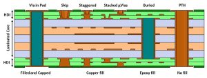
For dense 8-layer designs, via-in-pad, blind vias, buried vias, or microvias may be considered where appropriate and supported by the manufacturer’s process capabilities.
8. Core and Prepreg Selection
The core and prepreg materials determine dielectric thickness, dielectric constant, mechanical stability, and part of the impedance characteristics.
Their selection should account for:
- Target board thickness
- Required impedance
- Copper weight
- Thermal requirements
- Mechanical requirements
- Manufacturing tolerances
- Material availability
The final stackup should use realistic material parameters supplied or verified by the PCB manufacturer.
Manufacturing Considerations for an 8-Layer PCB
An 8-layer design can be electrically excellent but still difficult to manufacture if fabrication constraints are ignored.
Stackup Symmetry
A balanced and symmetrical construction is generally preferred for multilayer PCB fabrication because it helps control mechanical stress and reduce the risk of warpage.
Copper distribution, dielectric thickness, and material construction should be considered together.
Copper Thickness
The required copper thickness should reflect both electrical current requirements and manufacturing capabilities.
Thicker copper can improve current-carrying capacity and heat spreading, but it can also affect etching, trace geometry, via fabrication, and manufacturing cost.
Layer-to-Layer Registration
As layer count increases, registration becomes increasingly important.
Manufacturing processes must maintain appropriate alignment between:
- Internal copper layers
- Drilled holes
- Vias
- Pads
- Outer-layer features
A capable PCB Manufacturing partner should have appropriate multilayer registration and inspection processes.
Manufacturing Tolerances
Controlled impedance and fine-pitch structures depend on consistent manufacturing tolerances.
Designers should therefore communicate critical requirements to the manufacturer before production rather than relying exclusively on nominal CAD dimensions.
Production Lead Time
An 8-layer PCB normally requires more fabrication steps than a simple 2-layer or 4-layer board.
Depending on materials, copper thickness, via technology, surface finish, impedance requirements, and order quantity, production lead time can vary significantly.
Early communication with the manufacturer can help reduce unexpected delays.
Advantages of an 8-Layer PCB Stackup
Improved Signal Integrity
Multiple reference planes and carefully positioned signal layers provide more opportunities to create controlled return paths and isolate sensitive signals.
Greater Routing Capacity
Compared with lower-layer-count boards, an 8-layer PCB provides substantially more routing space.
This is particularly useful for designs containing:
- High pin-count processors
- DDR memory
- High-speed interfaces
- Multiple power domains
- Dense connectors
- Complex peripheral circuits
Better EMI Management
Appropriate ground-plane placement and signal-layer isolation can reduce unwanted electromagnetic coupling.
This is especially important in high-speed digital, RF, telecommunications, automotive, and industrial electronics.
Better Power Distribution
Dedicated power and ground structures can reduce distribution impedance and support stable power delivery to complex electronic systems.
Greater Mechanical Stability
A properly balanced multilayer structure can provide good mechanical rigidity and dimensional stability.
The additional copper and dielectric layers also contribute to the overall structural strength of the board.
Higher Design Density
An 8-layer board allows engineers to integrate more functionality into a relatively compact PCB area without relying entirely on a much larger board footprint.
8-Layer PCB Applications
8-layer PCBs are widely applicable to electronic systems where routing density, electrical performance, and physical size must be balanced.
Aerospace and Defense Electronics
Aerospace systems can require compact, reliable, high-density electronics with carefully controlled signal integrity and power distribution.
Wireless Communication
Wireless and telecommunications equipment often combines high-speed digital processing with RF circuitry, making grounding, isolation, impedance control, and EMI management important.
Medical Electronics
Medical imaging, monitoring, diagnostic, and other sophisticated electronic systems may require multilayer boards to accommodate dense interconnections and reliable power distribution.
Computer and Control Systems
Processors, memory devices, high-speed interfaces, and multiple peripheral circuits can require additional PCB layers to provide sufficient routing capacity.
Consumer and Wearable Electronics
Advanced smartphones, tablets, wearable devices, and other compact electronics may use multilayer PCB structures to accommodate dense component placement and high-speed interfaces.
Industrial and Automotive Electronics
Industrial controllers, vehicle electronics, communication systems, and advanced control units can also benefit from the additional routing and reference-plane capability of an 8-layer PCB.
8-Layer PCB Stackup vs. Lower-Layer PCBs
| Feature | 2-Layer PCB | 4-Layer PCB | 6-Layer PCB | 8-Layer PCB |
|---|---|---|---|---|
| Routing capacity | Low | Moderate | High | Very high |
| Signal isolation | Limited | Good | Better | Excellent when properly designed |
| Reference planes | Limited | Good | Multiple | Multiple |
| High-speed design capability | Limited | Good | Very good | Excellent |
| Design complexity | Low | Moderate | High | High |
| Manufacturing cost | Low | Moderate | Higher | Higher |
| Typical use | Simple electronics | General electronics | Complex electronics | High-density complex systems |
The increase in layer count should be justified by actual electrical, routing, mechanical, and manufacturing requirements.
How to Optimize an 8-Layer PCB Stackup
A practical optimization process can follow these steps:
- Define electrical requirements — Identify signal speeds, impedance targets, power domains, and sensitive circuits.
- Estimate routing requirements — Determine whether four or more signal layers are needed.
- Assign reference planes — Provide suitable ground and power references for critical signals.
- Develop the preliminary stackup — Define layer order, dielectric thickness, copper weight, and material construction.
- Run impedance calculations — Verify that trace geometry can achieve the required impedance.
- Review return-current paths — Ensure high-speed signals have continuous reference planes.
- Evaluate thermal requirements — Consider copper planes, thermal vias, and high-power components.
- Perform DFM review — Confirm that the proposed stackup can be manufactured reliably.
- Confirm the stackup with the PCB manufacturer — Adjust material and fabrication parameters based on actual manufacturing capabilities.
- Finalize the PCB Design — Route the board only after the stackup and critical manufacturing parameters are established.
Conclusion
An 8-layer PCB stackup is more than simply adding eight copper layers to a circuit board. Its real value comes from the careful interaction between signal layers, ground planes, power planes, dielectric materials, vias, and copper structures.
A well-designed stackup can provide greater routing capacity, improved signal integrity, better power distribution, reduced crosstalk, stronger EMI control, and improved mechanical stability. However, these benefits depend heavily on correct layer assignment, reference-plane continuity, impedance control, thermal management, and manufacturability.
For successful PCB Design, engineers should establish the stackup early and consider signal integrity, power integrity, DFT, thermal requirements, and DFM together. During PCB Manufacturing, the selected materials, copper thickness, layer registration, via technology, and manufacturing tolerances must be compatible with the proposed design.
Kingda can work with customers from stackup development through fabrication, helping engineers evaluate multilayer construction, material selection, impedance requirements, routing constraints, and manufacturing considerations for reliable 8-layer PCB production.