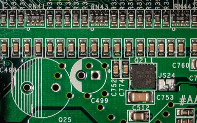
BGA PCB Surface Finish Risks and How to Prevent Defects
Ball Grid Array packages place their solder balls underneath the component body. That layout packs many connections into a small footprint, but it also hides every joint after reflow. Visual inspection cannot confirm what happened under the package. The surface finish on the PCB pads becomes one of the few controllable variables that decide whether those hidden joints form correctly. A finish that leaves uneven solder height can offset the package during placement.
A finish that wets poorly can leave weak or open joints. Reviewing the finish choice before tooling is released costs little and prevents expensive rework later.
The risk grows as pitch shrinks. Fine-pitch BGA packages leave very little room between adjacent balls. Small differences in pad height or solder volume can shift the balance of the whole array. Engineers should treat surface finish as part of the assembly process, not as a separate purchasing decision. The finish interacts with solder paste, stencil design, placement force and the reflow profile. When one of these changes, the others should be checked again. This connected view is what keeps a build predictable from lot to lot.
Why BGA Pads Demand Flatness
Each solder ball must land on its pad and collapse evenly during reflow. If one pad sits higher than its neighbor, the package may tilt slightly. Balls over high pads compress first and form a sound joint. Balls over low pads may not touch the paste at all. The result is a mix of strong and weak connections under one component. Because the joints are hidden, this condition often survives inspection and appears later as an intermittent fault.
Flat, consistent pad surfaces give every ball the same starting condition. That consistency matters more than any single material property.
Pad height variation comes from several sources. The base copper thickness varies across the panel. The finish itself adds a layer whose thickness may not be uniform. Plating and etching steps also affect how level the final pad becomes. A finish that deposits uneven solder on the pad transfers that unevenness directly into the joint. A finish that adds a thin, uniform layer keeps the pad geometry closer to the design intent.
Buyers should ask how the supplier controls finish thickness across the panel, not just at one test point. Uniformity across the array is the number that matters.
How HASL Affects BGA Joints
Hot Air Solder Leveling coats exposed copper with solder and blows excess away with hot air. The process is mature, widely available and suits many conventional boards. On BGA pads, however, the air knife does not leave a perfectly level surface. Some pads end up with thin solder, others with thick solder, and some show a concave shape. These differences are small in absolute terms but large relative to a fine-pitch ball.
When the package settles, the higher pads carry the load first. Solder volume then varies from joint to joint across the same component.
The consequences appear in two directions. Pads with too little solder can produce weak or open joints after reflow. Pads with too much solder can push molten material toward a neighbor and create a bridge. Both defects sit under the package and resist optical inspection. For coarse-pitch BGA packages, HASL may still work when the process is tightly controlled. For fine-pitch and high-density arrays, the flatness margin becomes too thin to rely on. Engineers should match the finish to the pitch rather than assume one finish fits every design.

Open Joints and Bridging Risks
An open joint forms when a ball fails to connect to its pad. Uneven pad height is one cause, and insufficient paste deposition is another. The two often combine. A low pad receives less paste, sits farther from the ball, and never wets during the reflow window. The joint may look acceptable under X-ray at first and fail later under thermal cycling. Intermittent connections are especially costly because they escape functional test and surface in the field.
Preventing them starts with a level pad surface and a verified paste volume on every pad in the array.
Bridging is the opposite failure. Excess solder on one pad flows into the gap to its neighbor during melt. At fine pitch, that gap is narrow, so even a modest surplus can close it. A bridge creates a short between two nets and may damage components when power is applied. Finding it requires X-ray or electrical test, because the joint is hidden. Both open and bridge defects trace back to the same root: inconsistent solder volume per pad.
A flat finish removes one major source of that inconsistency before the board reaches the printer.
ENIG for Fine-Pitch Arrays
Electroless Nickel Immersion Gold deposits a thin, uniform gold layer over nickel. The resulting pad is flat and resists oxidation during storage. That flatness helps the package sit level and helps paste release behave the same way on every pad. ENIG is widely used for fine-pitch BGA, QFN and chip-scale packages for this reason. The gold surface also offers good solderability after reasonable storage periods. For designs where coplanarity drives yield, ENIG gives a more predictable starting surface than solder-based finishes.
ENIG still needs process control. The nickel and gold thickness must stay within the supplier’s window, and bath chemistry must be maintained. Poor control can affect solder joint strength, so buyers should request thickness data with the lot. The finish also costs more than HASL, which matters on cost-sensitive boards. The decision should weigh pitch, reliability target and volume together.
Where the array is fine-pitch and the product is expensive, the added cost is usually small against the cost of a field return. Our SMT PCB assembly team reviews finish and stencil choices together during the DFM check.
OSP as a Flat Alternative
Organic Solderability Preservative protects bare copper with a thin organic film. It adds almost no height, so the pad stays essentially flat. That makes OSP attractive for fine-pitch BGA work where coplanarity is the main concern. The process is simple and compatible with lead-free reflow. It also avoids the solder-coating variation that causes trouble with HASL. For many high-density designs, OSP provides a workable flat surface at a lower cost than ENIG. The tradeoff lies in handling and storage rather than in flatness.
OSP offers limited protection against repeated thermal excursions and multiple reflow cycles. The film can degrade, so the number of passes matters. Storage conditions and shelf life also need attention, because the coating protects copper only while it remains intact. Boards that sit in a warehouse for months may need a bake or a re-screen before assembly. Buyers should confirm the reflow cycle count and the storage plan with the fabricator. When those conditions are met, OSP performs well on BGA arrays.
Our quality management process tracks finish, storage and reflow records together.
Selection Factors for Buyers
Pitch is the first filter. As ball spacing shrinks, flatness becomes more important than finish cost. Pad size and geometry come next, and the footprint should follow the component maker’s land pattern. Surface flatness across the whole array should be confirmed, not assumed from a single coupon. The assembly process must also match the finish, including paste type, stencil aperture and reflow profile. Finally, storage and expected product life shape the choice between ENIG and OSP. Each factor should be documented before the first article is built.
The reflow profile deserves its own review. A profile that works on one finish may not suit another, because wetting behavior differs. Engineers should confirm the soak time, peak temperature and time above liquidus against the paste supplier’s data. Solder paste inspection at the printer catches volume drift before placement. Placement accuracy then decides whether each ball meets its pad centered. After reflow, X-ray and electrical test close the loop. For teams moving a design to volume, high-volume PCB assembly planning should include these checks from the start.
Process Controls That Reduce Risk
A finish choice alone does not guarantee good joints. The printer must deliver consistent paste volume to every pad in the array. Stencil thickness and aperture design control that volume, and both should be verified against the pad geometry. Solder paste inspection gives a measurement per pad rather than a visual impression. Placement force and alignment decide how the balls contact the paste. The reflow profile then determines how the joints form and collapse.
Each step feeds the next, so a change in one should trigger a review of the others.
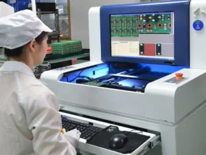
Inspection should match the risk. Automated optical inspection catches placement errors and visible defects around the package. X-ray reveals voids, bridges and open joints under the body. Electrical test confirms connectivity, and functional test proves the board works under power. Records from each step let engineers trace a defect back to its cause. When a batch fails, the data shows whether paste, placement or reflow drifted. That feedback loop is what lowers defect rates over time. As a routine part of every order, buyers should request these records.
Verification Before Release
Before the first production lot, engineers should confirm the finish specification in writing. The drawing should state the finish type and the thickness window. The process sheet should record the bath or coating parameters used. The inspection plan should list how flatness and thickness are checked. First-article approval should include X-ray of the BGA array and electrical test results. Any deviation should be closed before the next build starts. For prototypes, the same checks apply at smaller scale, and rapid PCBA prototyping can reveal pad and paste issues early.
The takeaway for buyers is simple. Match the finish to the pitch, then verify it with data. Ask for thickness records, flatness checks and first-article X-ray results before approving the lot. Confirm that paste volume and reflow profiles are measured, not assumed. Keep those records with the lot so a later field return can be traced quickly. Where the array is fine-pitch and reliability matters, ENIG or OSP usually beats HASL on flatness.
The finish is one decision among several, and it should be reviewed alongside stencil, placement and PCBA testing coverage.