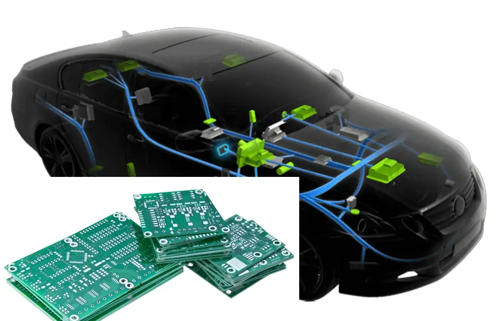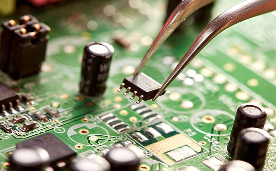
PCB Data Matrix Marking Verification: Reading It Back Buyers and engineers often focus on the finished product and forget the production line behind it. In practice, most field failures can be traced back to process decisions made during assembly. Understanding PCB data matrix marking verification gives you a practical advantage…
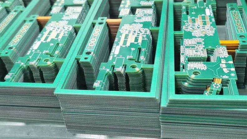
PCB Laser Marking of A QR Code: A Code on the Board Electronics manufacturing has become a discipline of small details. Solder paste volumes, placement accuracy, temperature profiles and inspection limits all add up to the final result. This guide looks at PCB laser marking of a QR code from…
PCB Breakaway Tab Width Selection: Holes and Tabs Buyers and engineers often focus on the finished product and forget the production line behind it. In practice, most field failures can be traced back to process decisions made during assembly. Understanding PCB breakaway tab width selection gives you a practical advantage…
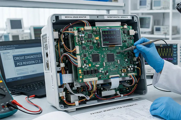
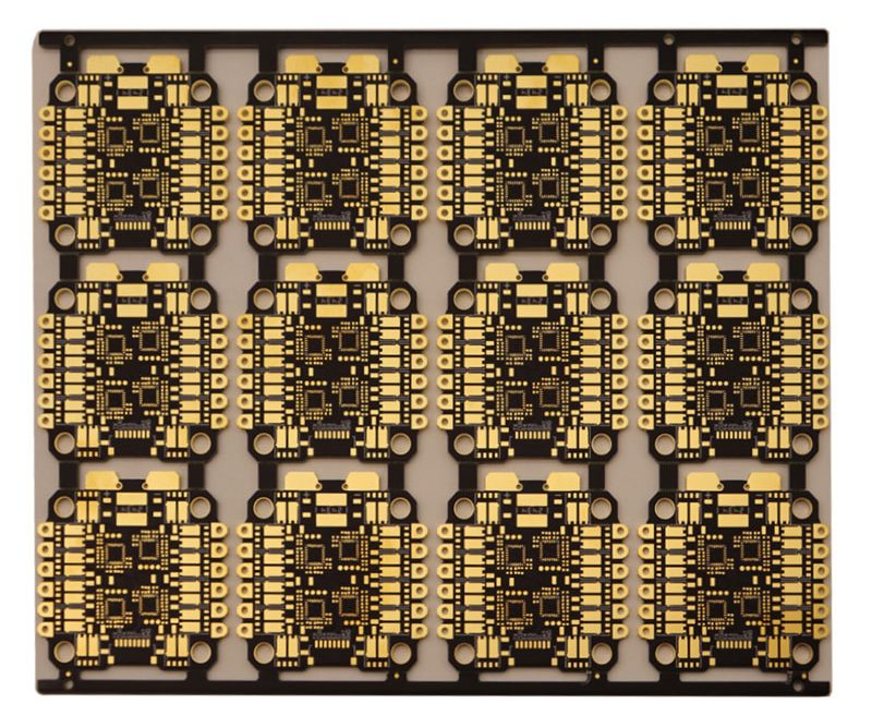
PCB Panel Array Design Rules: Fitting the Array Buyers and engineers often focus on the finished product and forget the production line behind it. In practice, most field failures can be traced back to process decisions made during assembly. Understanding PCB panel array design rules gives you a practical advantage…
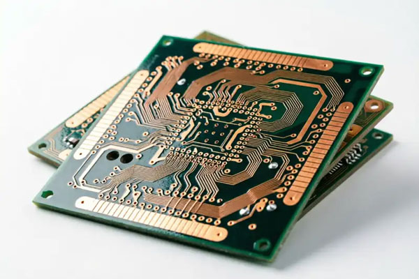
PCB Global and Local Fiducial Marks: Getting the Vision Right Modern electronics depend on boards that are assembled correctly the first time. Every product – a phone, a charger, a medical instrument or an industrial controller – relies on thousands of solder joints that must conduct current for years. This…
Calculating Trace Width for Current and Temperature Rise Trace width is decided by two questions that pull in opposite directions. The trace has to carry its current without getting too hot and without dropping too much voltage, which pushes the width up; and the routing has to fit into the…
PCB Tooling Hole Position on the Panel: Locating the Panel Buyers and engineers often focus on the finished product and forget the production line behind it. In practice, most field failures can be traced back to process decisions made during assembly. Understanding PCB tooling hole position on the panel gives…
PCB Router Versus Punch Tooling: Two Ways to Cut Out Electronics manufacturing has become a discipline of small details. Solder paste volumes, placement accuracy, temperature profiles and inspection limits all add up to the final result. This guide looks at PCB router versus punch tooling from the perspective of a…
PCB V Score Depth Setting: Depth of the Groove Electronics manufacturing has become a discipline of small details. Solder paste volumes, placement accuracy, temperature profiles and inspection limits all add up to the final result. This guide looks at PCB v score depth setting from the perspective of a PCBA…
Through-Hole Pad and Hole Size Design Through-hole parts are easier to justify than to design. The decisions that matter are small numbers — the hole diameter, the land around it and the distance between two holes — and each of them is a compromise between making the part easy to…