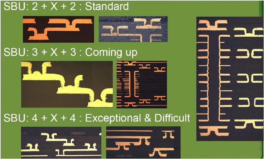
Via Stub Effects and Back Drilling at High Frequency A via that connects two layers also connects to every layer below, whether those layers need the connection or not. The unused portion is a stub, and at high frequency it behaves like a small antenna attached to the signal path.…

PCB Silkscreen Improvement: Getting Better Each Lot Buyers and engineers often focus on the finished product and forget the production line behind it. In practice, most field failures can be traced back to process decisions made during assembly. Understanding PCB silkscreen improvement gives you a practical advantage when you choose…
PCB Silkscreen Handover: Passing It On Buyers and engineers often focus on the finished product and forget the production line behind it. In practice, most field failures can be traced back to process decisions made during assembly. Understanding PCB silkscreen handover gives you a practical advantage when you choose a…
PCB Silkscreen Timing: How Long It Takes Buyers and engineers often focus on the finished product and forget the production line behind it. In practice, most field failures can be traced back to process decisions made during assembly. Understanding PCB silkscreen timing gives you a practical advantage when you choose…
PCB Silkscreen Environment: Where It Happens Electronics manufacturing has become a discipline of small details. Solder paste volumes, placement accuracy, temperature profiles and inspection limits all add up to the final result. This guide looks at PCB silkscreen environment from the perspective of a PCBA factory floor, covering controlling the…
High Tg Material Selection Guide A high tg laminate is one whose glass transition temperature is well above the ordinary range. Above that temperature the resin stops behaving as a glass and becomes more compliant, so its expansion rises sharply and its mechanical stiffness falls. A material with a higher…
Solder Paste Volume Control In SMT Printing Solder paste volume is the single number that links the printing process to the quality of the joint. The volume of paste printed into an aperture, less what is lost during reflow, becomes the solder fillet, and a fillet that is too small…
Via Tenting Versus Plugging On PCB Assemblies A via is a hole through the board, and leaving it open creates problems: solder can wick down the barrel during reflow, flux can be trapped inside, and contamination can enter the hole over the life of the product. Tenting and plugging are…
Annular Ring Requirements For Plated Holes The annular ring is the width of copper that surrounds a drilled hole on the pad. It is the material that connects the plated barrel to the conductor on that layer, and it is the part of the pad that has to survive drilling,…
PCB Silkscreen Traceability: Following One Board Electronics manufacturing has become a discipline of small details. Solder paste volumes, placement accuracy, temperature profiles and inspection limits all add up to the final result. This guide looks at PCB silkscreen traceability from the perspective of a PCBA factory floor, covering tracing silkscreen…