Seven Steps of PCB Design: From Library to Output A board that is designed twice costs twice as much, and most of the rework comes from skipping a step that takes an hour. The seven stages below are the ones that catch the mistakes while they are still cheap to…
PCB Gold Finger Plating Thickness: How Much Gold Buyers and engineers often focus on the finished product and forget the production line behind it. In practice, most field failures can be traced back to process decisions made during assembly. Understanding PCB gold finger plating thickness gives you a practical advantage…
FR4 and Aluminum Substrates: Where the Process Differs An aluminum substrate and a glass reinforced epoxy board are both called printed circuit boards, but the process that makes them differs from the first operation. The metal has to be drilled differently, and the insulation between the conductor and the base…
Kirkendall Voids: A Failure Mechanism Inside Solder Joints Every solder joint is a metallurgical system, not a frozen droplet of metal. Copper and tin continue to react long after the iron has cooled, and the interface between them keeps changing for the life of the product. Under the right combination…
PCB Rework of Coated Boards: Getting Back In Electronics manufacturing has become a discipline of small details. Solder paste volumes, placement accuracy, temperature profiles and inspection limits all add up to the final result. This guide looks at PCB rework of coated boards from the perspective of a PCBA factory…
PCB Masking for Coating: Protecting What Must Stay Clean Buyers and engineers often focus on the finished product and forget the production line behind it. In practice, most field failures can be traced back to process decisions made during assembly. Understanding PCB masking for coating gives you a practical advantage…
Chip Wound Inductor Selection For DC-DC Converters A chip wound inductor is a wire coil wound on a magnetic core and housed in a surface mount body, and it is the component that stores energy in most switching converters. Unlike a multilayer or a thin film part, the winding is…
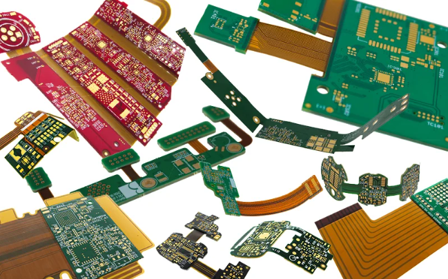
Flex Circuit 3D Folding And Bend Verification A flat layout is a poor representation of a folded flex circuit. The board may be drawn as a rectangle on the screen, while in the product it wraps around a battery, bends through a hinge or folds behind a display. The parts…
Ceramic Substrate Technology Trends For Power Ceramic substrates sit at the point where a circuit has to be electrically insulating, dimensionally stable and thermally conductive at the same time. Polymer laminates can satisfy the first two requirements and struggle with the third, which is why the ceramic option appears in…
PCB Warpage: Causes and Control Through Reflow Warpage is a change in the shape of a board that is measured against a flat surface. It shows up as a board that will not sit flat in a fixture, as a component that lifts, or as a solder joint that cracks…