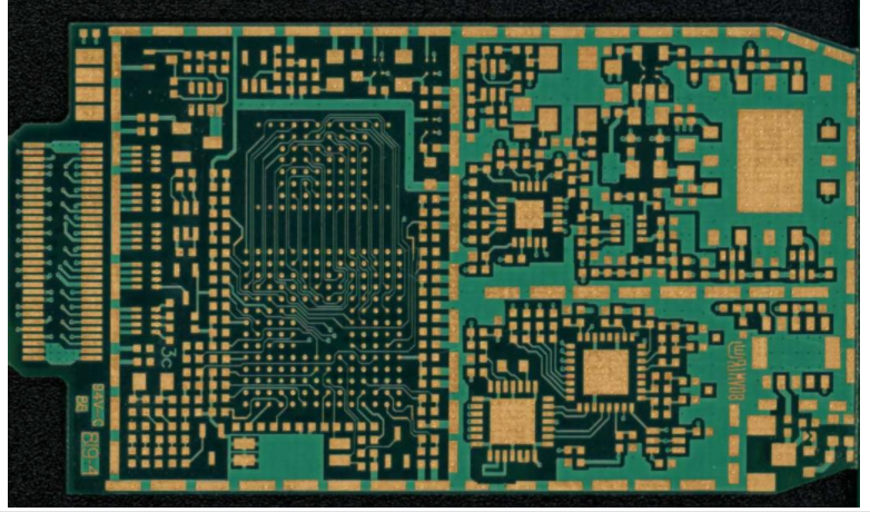
PCB Defect Pareto: Putting the Faults in Order Modern electronics depend on boards that are assembled correctly the first time. Every product – a phone, a charger, a medical instrument or an industrial controller – relies on thousands of solder joints that must conduct current for years. This article explains…
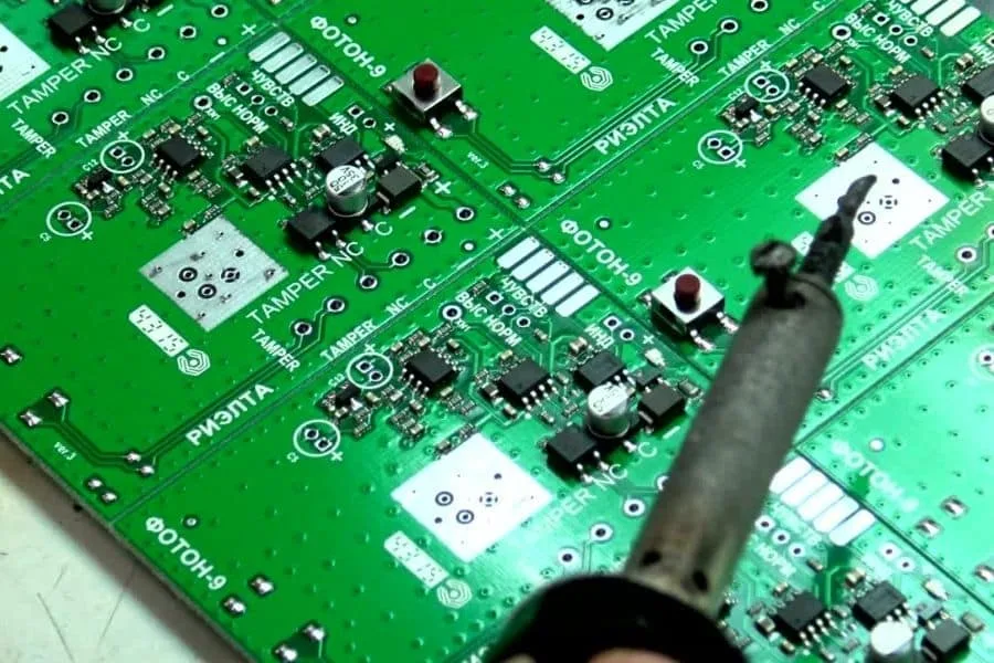
PCB 8D Report: Eight Steps to a Fix Electronics manufacturing has become a discipline of small details. Solder paste volumes, placement accuracy, temperature profiles and inspection limits all add up to the final result. This guide looks at PCB 8D report from the perspective of a PCBA factory floor, covering…
HDMI Interface ESD Protection Layout An HDMI interface carries several gigabit pairs, a set of control lines and a power pin through a connector that the user plugs and unplugs by hand. That combination of speed and human contact makes it one of the hardest interfaces to protect without degrading,…
Underfill for Board Level Reliability: When It Pays Off Underfill is a filled epoxy that is dispensed alongside a package and drawn under it by capillary action. It exists for one reason: to spread the stress that thermal expansion puts on solder joints across a larger volume of material. Used…
PCB Scrap Analysis: What Went in the Bin Modern electronics depend on boards that are assembled correctly the first time. Every product – a phone, a charger, a medical instrument or an industrial controller – relies on thousands of solder joints that must conduct current for years. This article explains…
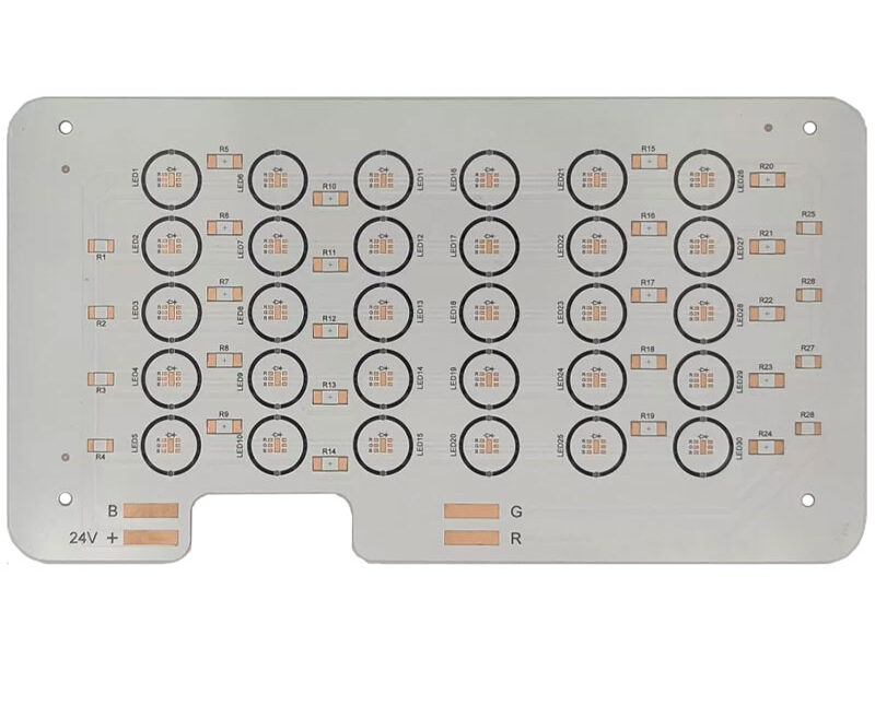
Cleaning Equipment and Bath Control for PCB Production Cleaning equipment is bought to remove what the soldering process leaves behind, and it only does that job when the chemistry, the mechanical action, the rinse quality and the drying step are all controlled together. A machine that is correctly sized and…
Trace Width Selection: Current, Rise and Impedance Trace width is one of the first decisions made in a layout and one of the least examined afterwards. Too narrow and the trace runs hot, drops voltage and may fail over time; too wide and routing space is wasted that dense areas…
Solder Paste Volume: Stencil Aperture and Print Parameters Most solder defects that appear at reflow were decided at the printer, and most printing problems are decided by the aperture in the stencil. The paste volume deposited on a pad is the single variable that predicts bridging, insufficient solder and voiding…
PCB Prototype Cost Factors You Can Control Prototype orders are priced differently from production because the fixed costs are spread over very few boards. Understanding which parts of the price are fixed, which scale with the board and which are optional is what allows a design team to reduce cost…
Gyroscope Sensor PCB Design Guide A MEMS gyroscope measures how fast something is rotating, and the number it reports is the difference between a real rotation and a set of error terms that are produced by the board it is mounted on. Temperature, vibration and mechanical stress all enter the…