AOI Programming and False Call Reduction in SMT Lines Automated optical inspection only earns its place on a line when the program behind it is trustworthy. A poorly tuned system floods operators with false calls until they start waving boards through, and at that point the machine protects nothing. Good…
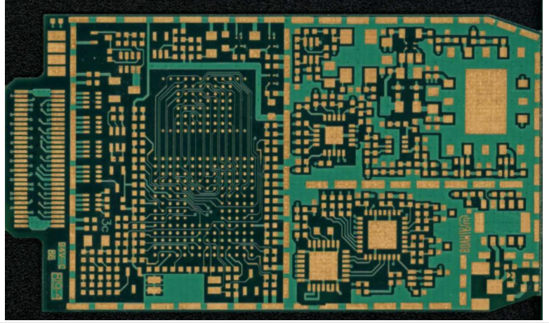
Four-Layer PCB Stackup vs Three Layers: Why Symmetry Wins Three-layer boards exist, but they are rare, and the reasons are mechanical and economic rather than electrical. A four-layer pcb stackup is the standard because it can be built symmetrically from standard materials, while three layers force a compromise. This guide…
PCB Edge Clearance Rules: Copper Near the Cut Buyers and engineers often focus on the finished product and forget the production line behind it. In practice, most field failures can be traced back to process decisions made during assembly. Understanding PCB edge clearance rules gives you a practical advantage when…
PCB Connector Pinout Assignment: Deciding What Goes Where Buyers and engineers often focus on the finished product and forget the production line behind it. In practice, most field failures can be traced back to process decisions made during assembly. Understanding PCB connector pinout assignment gives you a practical advantage when…
PCB Copper Pour Rules: Filling the Empty Space Electronics manufacturing has become a discipline of small details. Solder paste volumes, placement accuracy, temperature profiles and inspection limits all add up to the final result. This guide looks at PCB copper pour rules from the perspective of a PCBA factory floor,…
PCB Keep Out Zone Design: Space That Must Stay Empty Modern electronics depend on boards that are assembled correctly the first time. Every product – a phone, a charger, a medical instrument or an industrial controller – relies on thousands of solder joints that must conduct current for years. This…
Why Small Chip Components Rotate During Reflow A component that ends up rotated a few degrees after reflow looks like the result of a mechanical disturbance. Nothing touched the board, the placement machine reported no error, and yet the part has turned. The cause is almost always a force imbalance…
Gold Plating Thickness Specification for PCB Contacts Gold is used on circuit boards for two reasons: it does not oxidise, and it survives repeated mating. Both properties depend on how thick the gold is and on what lies beneath it, and the gold plating thickness that suits a low cost…
Conformal Coating Application and Masking Methods Guide A conformal coating is a thin polymer film that protects a finished assembly from moisture, dust, salt, and the small conductive debris that accumulates in service. It adds almost no weight and very little cost, yet it is often the difference between a…
PCB Sample Order Pricing: What a Small Order Really Costs A sample order is the smallest useful unit of a board programme. It proves the fabrication process, the fit and often the function, and its price is dominated by fixed charges rather than by the boards themselves. Understanding that structure…