Gold Finger PCB: Plating and Fabrication Guide A gold finger is the row of exposed contact strips along the edge of a board that plugs into a slot. The name comes from the plating, which is usually hard gold over nickel, and the reason for that plating is the same…

PCB Copper Weight vs Trace Width: A Current Sizing Guide Copper weight and trace width are two ways of solving the same problem: getting current from one place to another without overheating the conductor or dropping so much voltage that the load misbehaves. Copper weight sets how much metal is…
Automotive Control PCB: Design and Manufacturing Requirements A modern vehicle contains dozens of electronic control modules, and each of them has to work for a decade or more in an environment that would destroy consumer hardware. An automotive control PCB therefore differs from an industrial board not in the circuit…
Blind Slot and Open Slot Routing in PCBs: Depth, Tolerance and Sequence A slot in a printed circuit board is usually there for a mechanical reason: to seat a connector, to separate two circuits, to let air move or to give a daughter card somewhere to sit. Whether that slot…
PCB Junction Temperature Calculation: What the Die Actually Sees Buyers and engineers often focus on the finished product and forget the production line behind it. In practice, most field failures can be traced back to process decisions made during assembly. Understanding PCB junction temperature calculation gives you a practical advantage…
PCB Thermal Interface Pad Compression: Squeezing the Pad Right Electronics manufacturing has become a discipline of small details. Solder paste volumes, placement accuracy, temperature profiles and inspection limits all add up to the final result. This guide looks at PCB thermal interface pad compression from the perspective of a PCBA…
High Voltage PCB: Design and Fabrication Guide A high voltage board looks like an ordinary board that has been stretched. The traces are wider, the clearances are larger and there is a lot of empty laminate, and the empty space is the point. On a high voltage PCB the distance…
PCB Heat Pipe Interface: Moving Heat to the Case Modern electronics depend on boards that are assembled correctly the first time. Every product – a phone, a charger, a medical instrument or an industrial controller – relies on thousands of solder joints that must conduct current for years. This article…
PCB Vapor Chamber Interface: Spreading Heat Over a Plate Buyers and engineers often focus on the finished product and forget the production line behind it. In practice, most field failures can be traced back to process decisions made during assembly. Understanding PCB vapor chamber interface gives you a practical advantage…
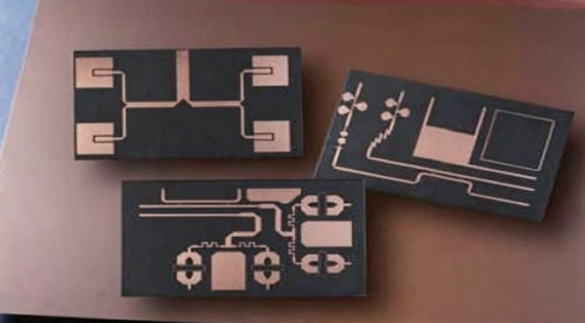
LNA RF Module PCB Design: Noise Figure and Grounding A low noise amplifier sits at the front of a receive chain and carries an unusual burden. Everything downstream adds noise on top of the noise it contributes, and the gain it provides cannot recover signal to noise ratio that has…