Burn In Board PCB Guide: Design, Materials, Process and Cost
What a Burn In Board Is
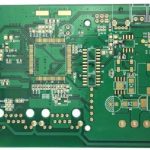
A semiconductor burn in board, often called a burn-in board, is a high performance PCB that carries chips through accelerated reliability testing. The board is installed inside a burn-in oven or an ATE system, holds the devices under test in sockets, and keeps them powered and running at elevated temperature for tens or hundreds of hours so that weak units fail early instead of failing in the field. Because it must survive repeated high temperature cycles, high current and continuous operation while holding precise impedance and signal quality, a burn in board is built to much tougher standards than an ordinary industrial PCB. These boards are used to screen AI chips, CPUs, GPUs, FPGAs, ASICs, DRAM, NAND flash, automotive MCUs, power semiconductors, medical chips and aerospace electronics.
Why Chips Must Be Burned In
Freshly packaged chips can hide defects that no final test at room temperature will reveal. Wafer fabrication defects, abnormal wire bonds, package stress, weak solder joints, electrostatic damage and material aging issues may only appear after the device has been stressed. If such parts reach a car, a data center or a medical system, the result can be a system crash, lost data, an automotive failure, an industrial shutdown or a medical device malfunction. Burn-in testing accelerates these latent failures by running devices at working temperatures of about 125 to 175 degrees Celsius under sustained power, high current, voltage stress and continuous cycling. Devices that survive the stress are far more likely to deliver consistent long term reliability, which is why burn-in is standard practice for high reliability chips.
How a Burn-In Board Works
The burn in board sits between the chip and the test system, distributing power and carrying test signals to every socket. In a typical run, the devices are loaded into sockets mounted on the board, the board is connected to the burn-in system, and the oven is heated to the programmed temperature. The system then supplies power, runs the test program, monitors current, voltage and functional state, and records the data for each device. Chips that drift out of specification are flagged and removed while the good units continue. Throughout the test the PCB itself must hold stable impedance, low signal loss and good thermal behavior, because a board failure would corrupt the very test it is supposed to perform.
Types of Burn-In Boards
Burn-in boards follow the package families they test. BGA burn-in boards support CPUs, GPUs and AI processors with dense routing and precise impedance. QFN boards serve automotive, industrial and consumer devices. CSP boards handle chip scale packages with very fine pitch routing. Flip chip boards are built for high speed, high frequency, high power devices and emphasize thermal management and signal integrity. Memory burn-in boards test DDR, LPDDR, HBM and NAND flash, and AI processor boards often combine high layer counts, heavy copper and complex heat spreading structures to deal with extreme power. Choosing the right board family matters because the socket footprint, routing rules and thermal budget are different for every package.

Materials for High Temperature Burn-In Boards
Material selection decides how long a board survives in an oven. High Tg FR-4 offers a good balance of cost, mature processing and stable performance for routine test conditions. Polyimide handles long term high temperature operation with excellent heat resistance, low thermal expansion, strong resistance to thermal shock and a long service life. Rogers high frequency laminates serve high speed chip testing with low dielectric loss, stable impedance and strong high frequency behavior. High CTI materials improve insulation for high voltage test environments, and ceramic PCBs bring high thermal conductivity, low expansion, dimensional stability and long term reliability to extreme temperature and high power applications. Each material is a trade between cost and the temperature, speed and voltage the test demands.
Design Essentials for Burn-In Boards
Designing a burn in board means balancing electrical, thermal and mechanical requirements. The laminate structure must survive sustained temperatures above 150 degrees Celsius without delamination or blistering, so the stack-up and prepreg system are chosen for heat. High speed interfaces need controlled impedance and careful differential routing so test data stays accurate. Thermal management uses thicker copper, thermal vias, large copper areas, copper coins or metal heatsinks to pull heat away from hot sockets. Because sockets are inserted and removed repeatedly, pads must be wear resistant and dimensionally stable. Signal integrity work includes matched differential pairs, complete return paths, minimal crosstalk, optimized power integrity and disciplined grounding, and warpage control requires balanced copper and matched materials across the panel.
How Burn-In Boards Are Manufactured
Production follows the same high reliability flow used for demanding multilayer boards. The process starts with an engineering review and DFM analysis, material confirmation, multilayer lamination, CNC drilling, laser micro via formation where HDI is used, copper plating of the holes, pattern transfer, surface finishing, AOI, electrical test, dimensional inspection and reliability verification. The capabilities that matter most are high layer count fabrication, fine line processing, precise hole position, controlled impedance, low warpage lamination and consistent copper thickness across the panel. A board that drifts in impedance or bows in the oven will produce bad test data no matter how good the chips are.
Surface Finishes for Repeated Socket Contact
The finish is critical because a burn in board sees thousands of socket insertions. ENIG provides a flat, oxidation resistant, solderable surface and is the most widely used option. Hard gold is chosen for frequent insertion environments because it wears extremely well and holds a stable contact resistance over a long service life. ENEPIG adds a palladium layer and delivers the best overall combination of solderability, wire bonding capability and contact reliability, making it the choice for advanced packaging and premium semiconductor test. Matching the finish to the socket type and the expected number of insertions prevents the contact degradation that quietly destroys test yield.
Standards for Burn-In Board Quality
Reliable burn-in boards are built and inspected against international standards. IPC-6012 Class 2 and Class 3 define rigid board performance requirements, IPC-A-600 covers bare board acceptance, IPC-2221 sets generic design rules, IPC-4101 specifies laminate and prepreg materials, and IPC-TM-650 provides the test methods used to verify properties. Environmental compliance with RoHS and REACH plus a quality management system such as ISO 9001 round out the requirement set. Specifying these standards gives chip manufacturers a consistent basis to qualify boards, compare suppliers and trust that a board rated for 175 degrees Celsius actually holds its properties there.

Common Failure Modes and Prevention
Burn-in boards fail in predictable ways when design or process control slips. Warpage and delamination appear when the stack-up or materials cannot take the heat, pads lift after repeated socket insertion, copper fatigues under thermal cycling, oxidation degrades contacts, sockets lose their grip, signals attenuate on long high speed routes and thermal cracks grow near heavy copper transitions. These problems are prevented by choosing a fabricator experienced with high temperature boards, balancing the stack-up and copper, using durable finishes, and completing a DFM review before release. A small investment in engineering review at the start prevents lost test time and corrupted reliability data later.
Burn In Board Cost
Burn in board cost depends on layer count, material grade, size, impedance control, finish, copper weight and quantity. Prototype boards of one to five pieces typically cost $250 to $900 each, small runs of ten to fifty boards run $180 to $550 each, and medium volumes of one hundred to five hundred boards fall to $90 to $280 each, with high volume production quoted per design. The main cost drivers are high Tg or polyimide materials, Rogers or ceramic laminates, HDI blind and buried via structures, impedance control, thick copper from 2 to 6 oz, ENEPIG or hard gold finishes and the reliability testing required. Because the total burn in board cost spreads across every chip the board qualifies, investing in a robust design usually pays for itself many times over.
Working With Your Burn-In Board Manufacturer
Burn-in boards are not commodity PCBs, so supplier selection deserves care. Ask your PCB manufacturing partner about maximum layer count, high temperature material experience, impedance capability, thick copper limits and available finishes before sharing your design. Review warpage control data and confirm that AOI, electrical test, X-ray and reliability checks are part of the standard flow. Work with the engineering team during PCB design and layout on the stack-up and thermal plan, and validate the finished boards with your PCBA testing group before they go into production service.
Burn In Board FAQ
Q1: What does a burn in board do? It holds chips under test at elevated temperature and power for long periods so that weak or defective devices fail early and never reach customers.
Q2: What temperature is used for burn-in? Most semiconductor burn-in runs at 125 to 175 degrees Celsius, with special applications going higher.
Q3: Which materials are best for burn-in boards? High Tg FR-4 suits routine testing, while polyimide, Rogers and ceramic laminates serve high temperature, high frequency and high reliability programs.
Q4: Which surface finish should a burn-in board use? ENIG covers most applications, hard gold is best for frequent socket insertion, and ENEPIG suits premium semiconductor and advanced packaging test.
Q5: Why are burn-in boards expensive? High grade materials, high layer counts, impedance control, thick copper and reliability testing all raise cost, but the expense is small compared with the value of reliable test data.
Conclusion
Burn in board PCBs are the workhorses of semiconductor reliability testing, carrying chips through the high temperature stress that exposes early failures before products ship. Their design combines heat resistant materials, controlled impedance, careful thermal management, durable finishes and low warpage manufacturing to an uncommon degree. Teams that qualify their PCB capabilities against the temperature, speed and socket requirements of their devices, and review the design with the factory early, will get boards that deliver trustworthy data for thousands of test hours.