Carbon Ink PCB and Package Substrate: Differences, Applications, and Manufacturing Technologies
What Is a Carbon Ink PCB?
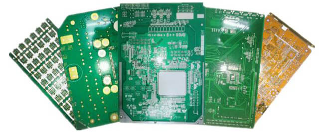
A Carbon Ink PCB is a type of printed circuit board that uses conductive carbon ink printed onto the PCB substrate to form conductive patterns. After the carbon ink is cured through a controlled heating process, it creates a durable carbon film layer that functions as an electrical conductor.
With the continuous development of the electronics industry, manufacturers are increasingly looking for cost-effective alternatives to traditional surface finishes such as gold plating. Carbon Ink PCB technology has become an effective solution, especially for applications requiring high durability, excellent wear resistance, and stable electrical performance.
Carbon ink contacts can withstand hundreds of thousands or even millions of repeated mechanical operations, making them widely used in membrane switches, keypads, control panels, and other electronic interfaces.
At Kingda, advanced PCB manufacturing technologies are applied to produce reliable Carbon Ink PCB solutions that meet the requirements of high-performance electronic applications.
How Does Carbon Ink Work on a PCB?
In a Carbon Ink PCB, carbon material acts as a conductive layer that connects different circuit points or functions as a resistor between circuits and components.
The production process mainly involves:
- Carbon ink formulation and preparation
- Screen printing of conductive patterns
- Thermal curing process
- Electrical resistance control
- Surface quality inspection
The carbon ink consists of fine carbon particles evenly distributed in a resin-based material. After printing and curing, these particles create a stable conductive pathway.
Compared with traditional metal conductors, carbon-based conductive layers provide:
- Excellent wear resistance
- Stable electrical conductivity
- High temperature resistance
- Lower manufacturing cost
- Long operating lifetime
Carbon ink can be applied to various PCB materials, including:
- FR-4 PCB
- FR-5 PCB
- Flexible PCB
- Rigid-Flex PCB
- PTFE-based laminates
- Polyimide and polyester substrates
Advantages of Carbon Ink PCB Technology
1. Excellent Wear Resistance
One of the biggest advantages of Carbon Ink PCB technology is its outstanding mechanical durability.
Unlike traditional metal contacts that may wear after repeated operation, carbon ink layers maintain stable performance even after extensive switching cycles.
This makes carbon ink suitable for:
- Automotive control panels
- Industrial equipment interfaces
- Consumer electronics buttons
- Medical devices
- Smart control systems
2. Cost-Effective Alternative to Gold Contacts
Gold plating provides excellent conductivity and corrosion resistance but significantly increases manufacturing costs.
Carbon ink provides a more economical solution while maintaining:
- Reliable conductivity
- Good contact performance
- Long service life
Therefore, many manufacturers choose Carbon Ink PCB designs as a replacement for expensive gold-plated contact solutions.
3. Excellent Electrical Performance
High-quality carbon materials provide:
- Low contact resistance
- Stable conductivity
- Good signal transmission
- Strong environmental resistance
The unique structure of carbon particles improves conductivity while maintaining mechanical flexibility.
What Is a Package Substrate?
A Package Substrate is a specialized substrate used to connect semiconductor chips with the main circuit board.
It acts as an electrical and mechanical bridge between an integrated circuit (IC) and a PCB board.
Unlike conventional PCBs, package substrates require extremely high manufacturing precision because they directly support advanced semiconductor packaging technologies.
A package substrate provides:
- Mechanical support for semiconductor chips
- Electrical connections between chips and PCBs
- Signal transmission paths
- Thermal management functions
Common package substrate applications include:
- CPU packaging
- GPU packaging
- Memory modules
- Mobile processors
- High-performance computing devices
Difference Between Package Substrate and PCB
Although both Package Substrate and PCB are used for electronic connection and component support, they have significant differences in structure, manufacturing process, and applications.
1. Different Functions
A PCB board is mainly used as a platform to connect multiple electronic components, including:
- IC chips
- Resistors
- Capacitors
- Connectors
- Sensors
The main purpose of a PCB is to provide electrical connections and signal transmission throughout an electronic system.
A Package Substrate, however, is mainly designed for semiconductor packaging. It connects a single chip or semiconductor device with the external PCB system.
Simply:
- PCB: Connects multiple electronic components.
- Package Substrate: Connects semiconductor chips to PCB systems.
2. Different Manufacturing Requirements
The manufacturing processes of PCB manufacturing and package substrate production are significantly different.
Traditional PCB production usually includes:
- Copper plating
- Circuit imaging
- Etching
- Drilling
- Lamination
- Surface finishing
- Electrical testing
Package substrate manufacturing requires much higher precision, including:
- Micro-patterning
- Fine-line routing
- Micro-via technology
- Advanced layer alignment
- High-density interconnection (HDI)
Because of these requirements, package substrates usually have finer circuits and stricter process control compared with standard PCB boards.
3. Different Material Structures
Common PCB materials include:
- FR-4 laminate
- High-frequency materials
- Polyimide materials
- PTFE materials
Package substrates often use advanced materials designed for semiconductor applications, such as:
- BT resin
- ABF materials
- High-performance dielectric materials
These materials provide:
- Better thermal stability
- Lower dielectric loss
- Higher dimensional accuracy
4. Different Application Fields
PCB applications include:
- Consumer electronics
- Automotive electronics
- Industrial equipment
- Communication systems
- Medical devices
- Aerospace electronics
Package substrate applications include:
- Advanced semiconductor packaging
- High-performance processors
- AI chips
- Memory devices
- Networking chips
Key Factors Affecting Carbon Ink PCB Manufacturing Quality
To ensure stable performance of Carbon Ink PCB, manufacturers need strict control throughout the production process.
1. PCB Design Optimization
The design of conductive carbon ink patterns directly affects:
- Electrical resistance
- Contact reliability
- Mechanical durability
Proper layout design helps achieve stable electrical performance and longer product life.
2. Selection of Screen Printing Materials
The quality of carbon ink materials has a direct impact on PCB performance.
Important factors include:
- Carbon particle size
- Resin compatibility
- Conductivity
- Adhesion strength
- Wear resistance
High-quality carbon ink ensures consistent electrical characteristics and reliable operation.
3. Manufacturing Process Control
Key production control points include:
Screen Printing Process
Accurate printing parameters are required to control:
- Ink thickness
- Pattern accuracy
- Surface uniformity
Curing Process
Proper curing temperature and time ensure:
- Strong adhesion
- Stable resistance values
- Improved durability
Surface Treatment
Surface treatment processes influence:
- Contact performance
- Environmental reliability
- Product lifetime
Conclusion
Both Carbon Ink PCB and Package Substrate play important roles in modern electronic manufacturing.
A Carbon Ink PCB provides a cost-effective, durable, and reliable solution for applications requiring repeated mechanical contact and stable conductivity.
A Package Substrate serves as a high-precision connection platform between semiconductor chips and PCB systems, supporting advanced electronic products such as AI processors, mobile chips, and high-performance computing devices.
As PCB technology continues to evolve, companies like Kingda continue to improve manufacturing capabilities, quality control systems, and advanced PCB solutions to meet the growing demands of the global electronics industry.