Chip Capacitor Flex Cracking: Stress Sources from Depaneling to Test
A chip capacitor fails in a way that incoming inspection cannot predict. The ceramic body cracks during depaneling, board handling, connector insertion or in-circuit test, and the damage appears later as a short or an open once the assembly is warm. The cause is mechanical, but it is introduced by process decisions that are usually filed under logistics. This article follows the stress path from panel singulation through assembly and test, and it gives the measurements that keep the cracks out of the finished board.
Where the Ceramic Body Fails
A multilayer ceramic capacitor is a stack of brittle dielectric layers terminated at each end, and its weakest plane is the interface where the ceramic meets the termination, because the two materials have different elastic moduli. Bending the board strains that interface, and once a crack starts it can travel through the electrode layers and create a conductive path that closes when the part warms up.
The quantity that matters is the strain applied to the body, not the force applied to the board. A 1.6 mm assembly deflected by roughly 1.5 mm over a 90 mm span is usually enough to crack the larger case sizes, and a 1206 or 1210 body fails at about half the deflection that a 0402 survives. Case size therefore sets the handling budget for the whole panel.
Singulation Stress from the Panel
V-score is the largest single contributor on most assemblies, because breaking a scored panel bends the material immediately beside the score and the strain field reaches several millimetres into the board. Keeping capacitors at least 5 mm from the break line, and never placing them with the long axis parallel to the score, removes most of that exposure. The panel details behind this are covered in our fabrication notes.
Router depaneling trades bending for local vibration and dust. A 2.0 mm carbide bit at 30 000 to 40 000 rpm and a feed of 25 to 40 mm per second cuts cleanly, but a dull bit or a single deep pass lifts the laminate and transmits load through the panel. Two or three shallow passes, with the bit replaced on a measured wear interval, keep the transferred stress low.
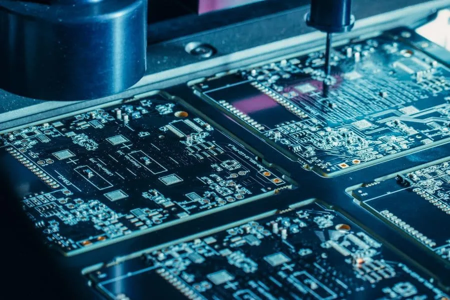
How the panel is supported under the cut matters as much as the tool. A routed edge taken with the panel held only at its outer rail lets the inner board move, and the movement appears as strain at the nearest component rather than at the cut.
Handling, Nozzles and Board Support
A placement nozzle applies a downward force to seat the part, and a nozzle that is oversized or a force setting that is too high presses the body onto the pad before the paste has anywhere to go. Vacuum pick-up forces of a few hundred grams are normal, but the limit belongs in the machine setup and should be re-checked after every nozzle change or feeder swap.
Support underneath matters just as much. A conveyor that lets a panel overhang more than about 25 mm, or a fixture that holds the board only at the edges, allows the centre to deflect under its own weight when the assembly is hot and soft. Tooling pins or a pallet supporting the area under the heavy components removes that movement, as described in our notes on warpage control.
Solder Joint Geometry and Stress Transfer
A tall solder fillet transfers more board strain into the ceramic, because the joint is stiff and grips the termination along its full height. Reducing the printed paste volume so the fillet reaches only part of the termination height lowers the load on the interface without weakening the electrical connection. The stencil aperture and paste volume that control this are discussed in our paste volume guide.
Pad geometry has the same effect. A land that extends well beyond the termination produces a fillet wrapping around the corner of the part, which is where flex cracks begin. Pad widths matched to the termination, with a land extension of 0.2 to 0.3 mm, give a fillet that is adequate and less damaging at the same time.
Rework and Hand Soldering
An iron tip puts a point load directly on the termination while a thermal gradient runs through the body. A tip at 350 degrees Celsius applied for three seconds to a small land is a common recipe and it works, but the tip must never rest on the ceramic, and the joint should be brought to temperature with preheat from the underside wherever the layout allows it.
Tweezers and hot air add a different load, because the part is gripped while the alloy is molten and any sideways movement shears the still-solid interior. Where a capacitor has to be replaced, the practical sequence is to add alloy, heat both ends evenly, lift the part with light force, and clean the land before the replacement is placed.
In-Circuit Test Force
A bed-of-nails fixture presses each probe onto a test pad with a spring force typically between 1.5 and 3 newtons, and on a dense board the sum is hundreds of newtons. If the support pins are not directly under the probe field, the board flexes between them and the deflection is concentrated at the components sitting over the unsupported span.
The measurable consequence is that capacitors crack during test and are then found at final inspection, where the process rather than the fixture gets the blame. Supporting every third or fourth probe position from underneath, and limiting the total applied force to a value verified with a strain gauge, stops the test from becoming a stress screen.
<img src="https://www.gopcba.com/wp-content/uploads/2024/09/RF-PCB.jpg" alt="Four point bend test fixture with a PCB under deflection” />
Strain gauges bonded beside the highest risk component turn the fixture setup into a measurement rather than an opinion. The peak strain during a full test cycle should be recorded for the worst board in the family.
Detecting Cracks That Cannot Be Seen
Automated optical inspection sees the top surface of the body, so a crack that opens at the termination interface or runs beneath the part is invisible to it. Capacitance measured at low frequency detects a partial crack as a small shift, and insulation resistance measured at rated voltage finds the ones that have already bridged the electrodes.
The reliable laboratory method is a bend test with the parts monitored electrically while the board is deflected. Four point bending at a controlled rate, with capacitance and resistance logged continuously, shows the deflection at which the first discontinuity appears, and that figure is the real process limit for the design. Our notes on test design cover the related monitoring setup.
Bend Test Method and Acceptance Criteria
A workable in-house method uses a span of 90 mm, a deflection rate of 1 mm per second, and a target deflection taken from the product requirement rather than from a generic figure. Boards are tested with components facing away from the loading nose for one condition and towards it for the other, because the two orientations load the ceramic differently.
Acceptance is stated as the number of parts that survive a stated deflection without a measurable change, so the sample has to be large enough to see a low failure rate. Ten boards says very little; thirty boards with a pass criterion of no electrical change gives a usable figure for a process that is supposed to be stable.
Drawing Notes and Process Ownership
The design side can remove much of the risk before the panel is ordered by writing four items onto the drawings: a 5 mm keep-out from every score line, the orientation of the larger case sizes, the maximum deflection the assembly must survive, and the handling class that applies to the board.
The process side owns the rest, and it is measured rather than assumed. Depaneling force, nozzle force, fixture support and test force are all recorded settings, and a change to any of them is a process change that requires the strain measurement to be repeated. That discipline is what holds the crack rate at zero after a fixture has been modified.
FAQ
Can a cracked capacitor pass functional test? Yes. A crack that has not bridged the electrodes measures normally at room temperature, and the failure appears later as a short after thermal cycling or moisture exposure.
Is routed depaneling always safer than V-score? No. Routing removes the bending load but replaces it with vibration and dust, so the bit condition and the number of passes matter as much as the method.
What deflection should the drawing specify? The value the product will actually see in handling and test, established by measurement on a sample assembly and then written as a requirement rather than left to the assembly house.