
More Layers Is Not Always Better: Choosing a PCB Layer Count
More layers is better is one of the oldest assumptions in board design, and it survives because a thicker stack-up does make some problems easier. The assumption breaks down as soon as cost, manufacturability and thermal behaviour are considered, because each additional layer pair adds process steps, reduces yield and lengthens the signal path that vias create. Choosing a layer count is a trade, not a ranking.
Why Layer Count Rose in the First Place
Layer count is a response to density, not a measure of quality. When two layers cannot carry the routing that the component pitch demands, the design adds layers because there is no other way to reach the pads. That is the honest reason most boards become multilayer. A board that can be routed on four layers without violating its electrical requirements does not become better by being built on eight.
The same logic explains the opposite trend. As integration improved, functions that once occupied several packages moved onto one device, and the routing demand on the motherboard fell. Boards that used to need many layers can now be built with fewer, because the nets that required them no longer exist.
What an Extra Layer Actually Costs
Each layer pair adds a lamination cycle, an imaging step, an etching step and a drilling operation, and each of those steps carries its own yield. The yields multiply, so the cost of a stack-up rises faster than linearly with the layer count. A board that was designed on eight layers when six would have met the requirements pays for the two extra layers on every unit, in material, in process time and in the scrap rate.
Manufacturing cost is not only the fabrication price. A higher layer count usually means a higher aspect ratio for the drilled holes, which affects plating uniformity and makes the smallest vias harder to produce reliably. Selecting a thinner core to keep the aspect ratio down has its own consequences for mechanical stiffness.

Signal Integrity Arguments for Fewer Layers
Counter-intuitively, a well-planned four-layer board can outperform a poorly planned eight-layer board. What matters for signal integrity is that every signal has a continuous reference plane beneath it, that the return path is not interrupted, and that the impedance is consistent along the trace. Those properties come from the arrangement of the layers, not from their number.
Adding layers without a plan can make matters worse. A stack-up with two routing layers adjacent to each other produces broadside coupling that a four-layer stack-up with a plane between the routing layers does not have. The additional layers then contribute cost and via stubs while the fundamental issue, an uncontrolled return path, remains.
The Electrical Requirements That Force More Layers
There are genuine reasons to increase the count. High pin-count devices with fine pitch escape routing need the area. Designs with multiple supply rails need planes to distribute them without sharing copper. Radio-frequency sections benefit from having a dedicated ground plane on each side of the signal layer. Impedance-controlled interfaces may require specific dielectric thicknesses that only a particular stack-up can provide.
In each case the requirement is specific and can be stated. A review that can articulate which net needs which plane will arrive at the minimum layer count that satisfies the requirements, which is usually lower than the first estimate.
Thermal and Mechanical Considerations
More copper is not automatically better for heat. A thicker stack-up with more internal planes spreads heat laterally, which helps a board with a few hot components spread over a large area, and it also conducts heat away from the component into the assembly more effectively, which can raise the temperature of neighbouring parts. The thermal design has to be evaluated as a system rather than inferred from the layer count.
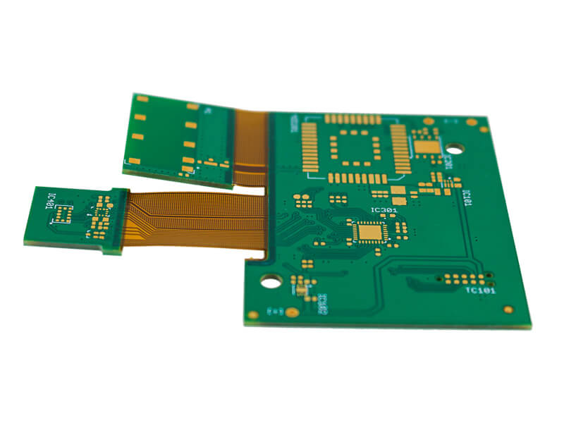
Mechanically, a conventional glass-fibre board should be flat and slightly flexible rather than brittle. A board that cracks when it is gently flexed, or one whose cut edge is rough and frayed, indicates a material or process problem that no layer count will fix. Rigidity comes from the total thickness and the material, not from the number of copper layers.
Choosing the Count in Practice
A workable method is to route the design as if it had one fewer layer pair than the current estimate, and see which nets fail to close. The failures identify the actual constraint: escape routing under a fine-pitch device, a supply plane that cannot be distributed, or an impedance requirement. Addressing that constraint specifically often allows the layer count to stay one pair lower than the initial guess, with the saving paid on every board built.
The choice should also be made before the layout starts. Changing the stack-up afterwards invalidates the impedance calculations, the via models and often the placement. Our layer assignment guidance covers the arrangement rules, the design and manufacturing cost reduction material explains where the fabrication cost sits, and the high layer count fabrication notes describe what changes when a stack-up becomes complex.
Where the Extra Layers Usually Come From
When a design ends up with more layers than expected, the cause is usually one of four things. The first is a component that was placed without considering its escape routing, so the fan-out under a fine-pitch device occupies an entire layer pair. The second is a power distribution scheme where every rail was given its own plane instead of being split on a shared plane. The third is a ground requirement that could have been met by one plane but was duplicated defensively. The fourth is a late addition, such as a second memory device or a radio module, that was routed through the existing layers rather than being declared as a new requirement.
Each of these is easier to resolve before the placement is fixed. Moving a large device to a different orientation, planning the power distribution on two planes instead of four, or allowing a modest amount of split-plane sharing can remove a layer pair without compromising the electrical performance. The review question is simple: for each layer, what requirement would fail if that layer were removed? If the answer is nothing specific, the layer is probably unnecessary.
FAQ
Does a higher layer count improve EMC performance? It can, but only when the extra layers are used to give signals a continuous reference. A stack-up in which every signal layer is adjacent to a plane will radiate less than one in which signal layers are adjacent to each other, and that arrangement is achievable at several layer counts. Adding layers without controlling the reference is more likely to add via stubs and coupling paths than to reduce emissions.
Is a four-layer board adequate for a modern design? For a large proportion of designs, yes. A four-layer stack-up with signal layers outside and power and ground planes inside gives every signal a reference plane and controlled impedance, which covers the majority of digital and mixed-signal boards. The cases that need more are driven by escape routing density, multiple supply domains or radio-frequency requirements rather than by a general perception that four layers is not enough.
How does gopcb help with stack-up selection? We review the proposed layer count against the routing demand and the impedance requirements before the layout is finalised, and we quote the effect of an additional layer pair on the fabrication price. Because the stack-up affects the drill aspect ratio and the plating process, deciding it early is the most effective way to keep both the cost and the yield predictable.