Clamp Diode Protection: Where the Current Goes After It Conducts
Two diodes on an interface, one to the supply and one to ground, look like a complete protection scheme on a schematic. An overvoltage is steered up to the rail and an undervoltage is steered down to ground, and the pin stays inside its rating. The transient, however, is not interested in the elegance of the drawing. Its current still has to travel through the diode, through whatever impedance is in series, and into a rail or a ground that has to absorb it.
If any part of that path has the wrong impedance, the wrong capacity or the wrong layout, the clamping point moves. Worse, the problem can be exported onto the supply rail and affect components that were never part of the interface.
A Clamp Diode Does Not Absorb the Voltage
When the input rises above what the clamping node allows, the diode conducts and diverts part of the current to the rail. The node voltage is then limited to a value that depends on the device characteristic, the transient current and the impedance of the loop. Those three are not constants, and the last two are properties of the board rather than of the component.
This is why a clamping voltage cannot be treated as a fixed number taken from a graph. The larger the transient, the longer the loop, and the higher the dynamic resistance of the device, the further the real node voltage departs from the static expectation. A protection scheme is only as good as the path that carries the diverted current away.

Why Series Impedance Is Part of the Protection
If the external source is strong and there is almost no impedance between it and the clamping node, the diode may see a very large peak current the instant it conducts. A series resistor, the source impedance itself, or another limiting structure is what keeps that current inside the range the diode and the protected circuit can tolerate.
A first estimate is straightforward: divide the voltage difference between the input and the clamping node by the total series impedance. The result is only a first estimate, because the transient source impedance, the dynamic behaviour of the diode, the pulse width and the parasitic elements all change it. The final answer comes from the device curves and from the waveform measured on the board, not from a single division.
Where the Current Ends Up Matters
An upper clamp injects current into the supply rail. If that rail is lightly loaded and the regulator cannot sink current, the rail voltage rises, and a transient that began at one input pin now travels through the power distribution network to reach other devices. The interface problem has become a system problem.
Three checks follow, and they belong in the design review. Trace where the clamped current goes and identify which component absorbs or consumes it. Check the ground return on the lower clamp, and confirm that it is short, low impedance and does not pass through a sensitive reference. Then check the ratings that actually apply: peak pulse current, dynamic clamping behaviour and the effect of repeated stress, rather than the static forward voltage that appears first in the datasheet.

Stronger Protection Can Degrade the Signal
A protection device adds junction capacitance, leakage and series parasitics to the node it protects. On a fast digital interface, capacitance slows the edge and creates an impedance discontinuity; on a high impedance analogue input, leakage and its temperature coefficient turn directly into measurement error.
Selection therefore cannot be a comparison of clamping capability alone. Operating voltage coverage, parasitic capacitance, leakage, dynamic clamping, package and the layout of the return path all belong in the same table. The acceptable values depend on the component selection, the interface rate, the input range and the absolute maximum ratings of the device being protected, and those limits are usually much tighter than the protection device datasheet suggests on its own.
Layout Decides Which Part the Transient Meets First
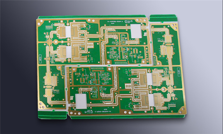
Energy entering from a connector should reach the protection device before it reaches anything else. If the protection point is close to the entry and its discharge loop is short, the transient current has little opportunity to find a path deeper into the board. If the trace branches to the core circuit before the clamp, part of the energy is already past the protection.
The working order is therefore: identify where the external energy enters, whether from a connector, a test point or a cable; place the protection device so the signal reaches it first with no branch ahead of it; make the path to ground or to the rail short and wide and keep it away from sensitive references; position any series current limiting component where it can genuinely constrain the clamp current; and for high speed or analogue interfaces, re-check the parasitic capacitance, leakage and impedance continuity that the protection introduces.
Four Questions for the Review
How much current? Estimate the peak from the worst case input and the total impedance, and state the pulse duration as well. Where does it go? Draw the complete loop for the upper clamp and for the lower clamp, including the rail and the ground return. Who absorbs it? Assign the stress to the clamping device, the rail, the ground return and the protected input separately, and check each one. Will it distort? Confirm whether the capacitance, leakage and placement of the protection device affect normal operation, particularly at the fastest edge rate the interface carries.
These questions also determine what has to be verified on the built board. A clamp that behaves correctly at the nominal supply but lifts the rail when the load is light is exactly the case that a simple bench check will miss, and it will appear in the field as a device failure with no obvious cause. The same discipline applies to the enclosures and harnesses around the board, since a cable routed outside the chassis will collect the transient and deliver it to the connector. Interface protection should therefore be part of the design review and part of the acceptance testing, which is why the test specification should state the transient conditions the board has to survive, not only a schematic convention.
FAQ
Can I rely on the internal protection diodes of a chip? They are intended for transient events during handling, not for repeated external transients, and their current rating is usually small.
How do I choose the series resistor? Size it so the peak current stays inside the clamp rating, then confirm that the resistor does not slow the signal beyond what the interface allows.
Does a protection diode need a dedicated ground return? At minimum it needs a short, low impedance return that does not share a sensitive reference path.
Why does the fault appear on another part of the board? Because the clamped current entered a rail and the rail carried it to other devices.
Summary
A clamp diode conducting is the beginning of the analysis, not the end of it. The protection is complete only when the current magnitude is limited, the discharge path is short and defined, the rail or ground that receives the current can absorb it, and the device has not degraded the signal it is supposed to preserve. Draw the path for both clamps, check who carries the stress, and the weak point in most interface protection designs becomes obvious before the boards are built.