Comparison of Immersion Gold and Electroplated Nickel Gold Pad Surface Finishes in PCB Wire Bonding Applications
Wire Bonding, as a mainstream interconnection technology in high-reliability packaging, places strict requirements on the physical and chemical properties of the metallization layer on PCB pad surfaces. Among them, pad surface roughness, gold layer purity, nickel layer density, interface diffusion behavior, and long-term thermal stability directly determine bonding strength, ball shear, pull strength, and reliability performance under high-temperature and high-humidity environments. Among many surface treatment processes, Electroless Nickel Immersion Gold, or ENIG, and Electrolytic Nickel Gold, or E-Ni/Au, are widely used because they combine solderability, oxidation resistance, and bonding compatibility. However, the two have essential differences in microstructure, growth mechanism, and service behavior.
Differences in Microstructure and Process Mechanism
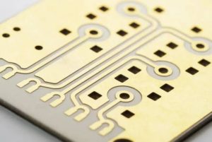
ENIG is an autocatalytic reduction reaction system. First, a high-phosphorus nickel layer with a thickness usually of 3 to 6 micrometers and containing 7 to 10 weight percent P is chemically deposited on the copper pad. Then, a thin gold layer of 0.03 to 0.1 micrometers is deposited on the nickel surface through a displacement reaction. This process requires no external current. The gold layer only covers the nickel surface. Due to displacement kinetics limitations, the gold layer is porous, has fine grains of less than 50 nanometers, and has low crystallinity. The nickel layer forms an amorphous or microcrystalline structure due to solid solution strengthening by phosphorus atoms, providing excellent copper diffusion barrier capability. In contrast, electroplated nickel gold requires acidic sulfate nickel plating first, with a thickness of 5 to 8 micrometers and P content less than 0.1 percent, followed by electrodeposition of a 0.1 to 0.5 micrometer gold layer from cyanide or cyanide-free alkaline gold plating solution. Electroplated nickel has a columnar crystal structure with relatively high internal stress of 80 to 120 MPa. The electroplated gold layer has coarse grains of 200 to 500 nanometers, is dense, has good ductility, and has better thickness controllability than ENIG.
Bonding Interface Reaction Kinetics and Intermetallic Compound Evolution
During Au-Al bonding, the gold ball undergoes plastic deformation under ultrasonic and thermal compression, breaking the oxide film. Al atoms diffuse into Au to form brittle intermetallic compounds such as AuAl2 and Au5Al2. Because the gold layer of ENIG pads is extremely thin and has micropores, rapid gold layer depletion occurs at the initial stage of bonding. Under typical bonding conditions of 225 to 250 degrees Celsius and 15 to 30 milliseconds, a 0.05 micrometer gold layer can be completely consumed at the first bond point, causing subsequent bond points to directly contact the underlying nickel and triggering Ni-Al IMC formation such as NiAl3. Its shear strength is only 60 to 70 percent of Au-Al IMC and is prone to purple plague failure. Because the gold layer of electroplated nickel gold is 0.2 micrometers or more and is continuous and dense, it can maintain gold layer integrity for 3 to 5 bond points, significantly suppressing nickel exposure risk. Measurements show that under the same bonding parameters, the coefficient of variation of ball shear force for electroplated gold pads is 4.2 percent, while that for ENIG is 9.8 percent, reflecting better interface reaction consistency.
Comparison of Thermal Cycling and Storage Reliability
In thermal cycling tests from minus 40 to plus 125 degrees Celsius for 1,000 cycles, ENIG samples showed microcracks at bond point edges after 500 cycles. XRD analysis confirmed that Ni3P phase precipitation along grain boundaries caused nickel layer embrittlement. At the same time, gold layer pores became moisture penetration channels. After 1,000 hours of 85 degrees Celsius and 85 percent relative humidity accelerated testing, Cu-Ni-O hydroxyl compounds were detected at the interface, causing a black pad failure probability of 12 percent. Electroplated nickel gold showed stronger thermal fatigue resistance. The low-phosphorus nickel layer has high grain boundary energy and is not prone to precipitating brittle phases. The electroplated gold layer has no pores and effectively blocks water vapor penetration. Under the same conditions, no interface corrosion was observed, and bond point shear force retention was greater than 95 percent. Measured data from a certain automotive-grade MCU module shows that the failure rate of Wire Bonding packaging using electroplated nickel gold in a 15-year life prediction model is 0.8 FIT, lower than the 3.2 FIT of the ENIG solution.
Process Compatibility and Manufacturing Challenges
ENIG is sensitive to front-end processes. If there are organic contaminants or uneven micro etching on the copper surface, it will cause nickel deposition rate fluctuations, leading to nickel hyper-corrosion or missed plating. The accumulation of phosphite in the plating solution will also reduce plating speed and coating uniformity. Strict monitoring of pH at 4.2 to 4.8 and temperature at 85 to 95 degrees Celsius is required. Although electroplated nickel gold has slightly lower requirements for pre-treatment, it faces two major bottlenecks. First, it is difficult to control internal stress in the nickel layer. Excessive tensile stress can easily cause pad warping and affect bonding alignment precision. Second, the gold plating solution is easily contaminated by copper ions from rack or fixture wear. When Cu2+ concentration is greater than 5 ppm, red-brown stripes appear in the gold layer, and bonding yield drops by more than 15 percent. In addition, the electroplating process requires dedicated rectifier power supplies, anode baskets, and automatic chemical addition systems. Equipment investment is about 40 percent higher than ENIG, but single batch processing capacity is increased by 3 times, suitable for mass production.
Cost and Supply Chain Adaptability Analysis
ENIG has a lower cost per unit area, about 0.8 to 1.2 US dollars per square meter, mainly because of low chemical consumption and no need for electric drive. However, its rework rate is high. The scrap rate caused by black pad problems reaches 3 to 5 percent, and hidden costs cannot be ignored. Electroplated nickel gold has higher material costs, about 2.5 to 3.8 US dollars per square meter. In particular, the unit price of cyanide-free gold plating solution is 2.3 times that of traditional cyanide systems. However, its first pass yield is stable at more than 99.2 percent, and it supports ultra-fine pitch pads of 50 micrometers or less, such as 0.8 mm pitch BGA, meeting advanced SiP packaging needs. In a high-end medical imaging equipment motherboard project, after the customer reduced pad size from 120 micrometers to 80 micrometers, the ENIG solution bonding failure rate rose to 22 percent, while electroplated nickel gold still maintained a 99.6 percent yield, verifying its process robustness advantage under miniaturization trends.
Selection Recommendations and Design Collaboration Points
For consumer applications with 50 or fewer bonding points, pad size of 100 micrometers or more, and operating temperature of 105 degrees Celsius or less, ENIG has cost and maturity advantages. However, for automotive electronics under AEC-Q200 Grade 1, aerospace, or long-term storage scenarios of more than 10 years, electroplated nickel gold must be preferred, and three design specifications must be followed. First, nickel layer thickness should be strictly controlled at 6.0 plus or minus 0.5 micrometers to balance diffusion barrier and stress. Second, the gold layer should use hard gold containing 0.1 to 0.3 percent Co, with Vickers hardness increased to 130 to 160 HV to enhance wear resistance. Third, the pad opening area must be solder mask defined to avoid green oil climbing and causing uneven bonding pressure distribution. In addition, it is recommended to clearly mark Ni/Au for Wire Bonding, Hard Gold, Co-doped, minimum 0.25 micrometers in the PCB Gerber file, and synchronously update pad size tolerance of plus or minus 2 micrometers in the stencil file to ensure precise execution at the PCB manufacturing end.
Gopcba provides professional PCB manufacturing, PCB assembly, prototype PCB assembly, low-volume PCB assembly, high-volume PCB assembly, SMT PCB assembly, through-hole PCB assembly, mixed-technology PCB assembly, flex PCB assembly, PCB design layout, components procurement, rapid PCBA prototyping, conformal coating, PCBA testing, box build assembly, wire cable harness assembly, medical PCBA, telecommunications PCBA, energy PCBA, industrial PCBA, artificial intelligence PCBA, Internet of Things PCBA, PCB capabilities, and PCBA capabilities. You can also visit our blog, learn about us, see why us, review our quality management, or contact us for more information.