Copper Foil Surface Profile and Adhesion in PCB Lamination
Copper foil is the conductor that carries every signal and every ampere on a printed circuit board, and the two industrial routes that make it produce materials with very different grain structures. The surface profile of that foil decides how firmly the laminate grips it, how much loss a high frequency trace shows, and how fine an etched feature can be before the process runs out of margin.
What Copper Foil Does in a Laminate
Foil arrives at the laminator as a thin continuous sheet that is bonded to resin under heat and pressure. Once bonded it becomes the copper that is imaged, etched and plated to form conductors, planes and pads, and its thickness is normally specified by weight in ounces per square foot rather than in microns.
The foil is not a passive sheet. Its treated side faces the resin and is engineered to grip it, while the opposite side faces outward and influences etching uniformity and plating appearance. Two foils of identical weight can behave very differently because the grain and the treatment are not the same.
Electrodeposited Foil and Its Grain
Electrodeposited foil is grown onto a rotating titanium drum from a copper sulphate bath. Copper deposits as columnar grains that grow outward from the polished drum surface, so the drum side is smooth and the growth side is rough. The route is fast and economical, which is why most rigid boards are built on it.
Because the grains are columnar, this foil tears more readily than the rolled product when it is flexed, and its rough side provides the mechanical key that the resin needs. Roughness is controlled by the deposition chemistry and by a subsequent treatment step that grows a nodular layer on the matte surface.
Rolled Annealed Foil and Its Uses
Rolled annealed foil is produced by rolling a copper ingot down to the required gauge and then annealing it to restore ductility. The grain is elongated in the rolling direction, so the sheet bends without cracking and survives many thousands of flex cycles. Flexible and rigid flex circuits are its natural home, as our notes on bendable circuit materials explain.
The rolled route costs more and is available in a narrower range of weights, and it is rarely used on thick rigid backplanes. Where a design mixes rigid and flex sections, the flex layers usually take rolled material while the rigid layers take electrodeposited material, and the two are laminated in a single press cycle.
How Surface Profile Is Created
Surface profile is what the resin sees when it wets the foil. On electrodeposited material the profile comes from the grain and from the nodular treatment layer applied to the bath side, with typical roughness values running from a few tenths of a micron up to about a micron depending on the grade.
Rolled foil starts smooth because the rolls polish it, so a treatment is applied to roughen it enough for bonding. That treatment is a copper oxide or a copper alloy layer, and its shape matters more than its average roughness, because the resin has to flow into the peaks rather than simply touch them.
Adhesion, Peel Strength and Oxide Treatment
Peel strength is measured by pulling a defined strip of foil away from the laminate at a fixed angle and rate. The value depends on the resin, the treatment and the lamination cycle, and it falls when the treatment is damaged by handling or by an oxide layer that has been allowed to hydrate before pressing.
Brown oxide and alternatives such as chemical tin or a silane coupling agent are chosen to suit the resin system. A treatment that works with epoxy may perform poorly with a hydrocarbon or a PTFE based material, so the foil and the resin have to be selected as a pair rather than independently.
Surface Roughness and High Frequency Loss
At high frequency the current crowds into the outer skin of the conductor, and a rough surface forces it to follow a longer path. The extra path length raises insertion loss, and the penalty grows with frequency, so a surface roughness that is harmless at a few hundred megahertz becomes a measurable penalty at millimetre wave. Our high frequency laminate guide covers the wider material picture.
Designers working above roughly ten gigahertz therefore ask for a low profile foil and often for a smooth rolled product. The trade off is adhesion, because a smoother surface bonds less readily, which is why treatment chemistry carries as much of the burden as the profile number itself.
Foil Thickness, Weight and Handling
Standard weights run from a quarter ounce through half, one and two ounces per square foot, with heavier material used for power and ground planes. Thin foil is fragile, since a half ounce sheet creases under a finger, and a crease becomes an etch defect or a pink ring after lamination. Copper balance on the inner layers changes how much of that thin material survives etching.
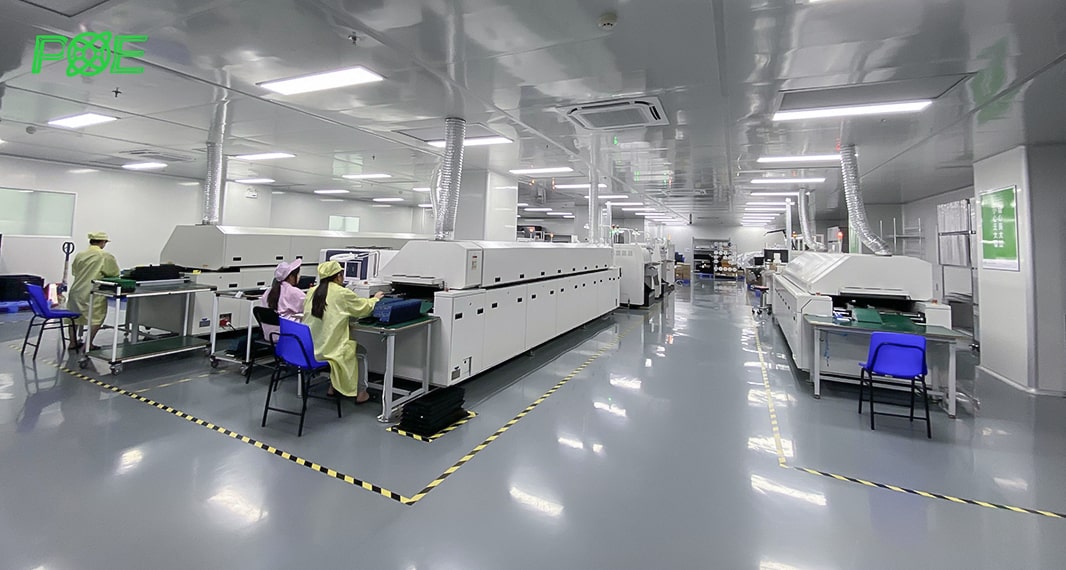
Handling therefore happens in a controlled area, and very light gauges are supplied on a carrier. Where the copper has to survive a heavy plating current, the designer may specify a heavier base foil rather than relying on plated copper alone to build the required cross section.
Choosing Foil for the Application
The choice follows from the electrical and mechanical requirement taken together. A flex tail needs fatigue life, a dense digital board needs fine etching, an antenna needs low loss, and a power board needs current capacity and heat spreading, and each of those pulls the decision in a different direction.
It is worth writing the requirement on the fabrication drawing instead of leaving it to the shop. A note that names the foil type, the weight and the profile class removes an assumption from the quotation, and it also settles which material qualification the finished board has actually been built against.
Inspection and What to Specify
Incoming material is checked against the certificate of analysis, and the practical measurements are weight, thickness, width, treatment appearance and, where the design is sensitive, roughness on a sample. Peel strength is verified on a coupon after lamination rather than on the incoming roll. A test coupon travelling with the panel carries those checks through production.
Specification writing is straightforward once the requirement is known: name the alloy, the route, the weight, the profile class and the treatment, then add the peel strength target and the test method. Anything left unnamed is chosen by the fabricator and may quietly change between orders. General guidance on laminate material properties helps set the rest of the stack-up around it.
FAQ
Is rolled annealed foil always better for flexible circuits? It is the usual choice, because its elongated grain survives repeated bending. Simple static flex sections are sometimes built on electrodeposited foil to save cost, but anything that flexes in service should not be.
Can a rough foil be used for a controlled impedance design? Yes, provided the roughness is known and the field solver accounts for it. Impedance itself shifts only slightly, but loss and phase respond differently, so the model should use the laminate supplier data rather than an ideal smooth conductor.
How does gopcb control foil selection? We record the foil type and weight on the stack-up drawing, keep incoming certificates with the job file, and verify peel strength on a coupon laminated with the production panel so the result describes the boards that ship.