Copper Thieving Density: Balancing Panels for Lamination and Warp Control
Copper thieving is not decoration. It is the copper added to areas that carry no signal so that the press sees a similar amount of metal across the panel, and the amount and distribution of that copper decide whether the lamination stays flat. The rules below come from press behaviour rather than from electrical requirements.
What Residual Copper Balance Means
Residual copper is the percentage of panel area still covered by copper after etching. A panel with 20 percent copper on one half and 70 percent on the other cures unevenly in the press, because the resin flows differently under each region and the two halves shrink by different amounts as the stack cools.
A practical target is to hold local residual copper within about 20 percentage points of the panel average when it is measured over areas of roughly 25 mm square. The check is made from the CAD copper layer before artwork is generated, and the density map is kept with the job so that the next revision starts from a known figure.
Pattern Choices: Dots, Grid and Solid Fill
Dot arrays of 0.5 mm to 1.0 mm pads on a 1.0 mm to 1.5 mm pitch are the most common thieving pattern because they etch cleanly and do not trap air in the press. A grid of crossing lines behaves in a similar way but leaves sharp interior corners where the etchant overhangs and the resist can lift.
Solid thieving is used only where a large area has to be brought up to the surrounding density, and even then it is broken by slots or dot rows. A solid patch bonded to a thin core acts as a stiffener and changes the warp signature in the opposite direction to the one that was wanted.
Placement Rules Around Features
Thieving copper is normally held back 0.50 mm from the panel edge and 0.25 mm to 0.30 mm from any functional copper, including traces, pads and plane borders. The clearance is wider than a normal trace spacing because the thieving carries no signal, and a short caused by it would be a defect with no electrical purpose at all.
On inner layers the same clearances apply, and thieving must be excluded from any area that will be routed away later. Copper within 0.30 mm of a rout path can smear into the cut and leave a burr that breaks free inside the assembly, and our fabrication notes treat that as a release item rather than a shop decision.
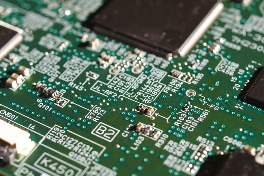
Thieving in the Press and the Effect on Resin Flow
During lamination the resin has to flow around the copper features before it gels. Where copper density is high and even, the flow is uniform and the dielectric thickness is predictable. Where density changes abruptly, the resin is starved in one area and rich in another, and the cured thickness can vary by 10 to 20 micrometres across the panel.
That variation reappears later as an impedance shift on controlled-impedance traces, because the trace width was modelled against a nominal dielectric height. Ten micrometres is enough to move a 50 ohm line by a few percent, which is why our laminate material data is quoted together with the balance figure.
Thieving as a Registration Aid
Because thieving is added symmetrically about the panel centre lines, it also steadies the dimensional behaviour of the panel from lot to lot. A panel that shrinks the same way each time can be scaled predictably in the drill programme, and registration improves without any change to the drill itself.
The pattern should be mirrored about the panel centre rather than repeated from one corner, so that residual asymmetry cancels instead of accumulating. Corner-anchored patterns drift with the sheet, and the drift is the same order of magnitude as the registration tolerance on a fine-pitch layer.
Warp Measurement and Acceptance
Warp is measured with the board resting on a flat granite surface, bow and twist being the maximum deviation from that surface expressed as a percentage of the diagonal or the edge length. The IPC-TM-650 method 2.4.22 procedure defines both the fixture and the calculation, so the figure is only comparable when the method is quoted with it.
Surface-mount assemblies commonly hold 0.75 percent for leaded devices and 0.5 percent for area-array packages. A panel that is inside those figures before assembly can still exceed them after reflow, so acceptance is applied after the assembly thermal cycle in fine-pitch products; our warpage control notes describe the fixture used for that check.

Interaction With Reflow and Carrier Fixtures
Boards with asymmetric copper heat unevenly and can bow during the reflow ramp, which is where the thieving design is really tested. The distortion at 240 degrees Celsius is a different number from the distortion at room temperature, and a panel can pass one and fail the other.
Where a carrier or pallet is used, the fixture should support the board at the same points the thieving stiffens it. Supporting a flexible area between two stiffened regions produces a local bend of its own, and that bend appears as a placement error on the side that is being assembled.
Cost and Yield Effects of the Pattern
Thieving costs nothing in material and almost nothing in etch time, but it does affect yield: unnecessary copper next to a fine-pitch layer increases the chance of a copper sliver and of a solder mask defect. The pattern should be no denser than the balance requires, and the density map is the evidence for that statement.
The other effect is scrap. Copper added outside the board outline is lost with the panel, so the pattern is normally applied only inside the assembly outline and along the break-off strips where the balance actually matters. On a panel with mixed board sizes this is also where the panel design is decided, since the thieving has to fit around the routing.
Documenting the Balance Check
The job file should show the density map, the panel average and the areas where the local figure deviates by more than the allowance. Recording the deviation together with the reason it was accepted is what makes the next revision faster than this one.
Fabrication notes should state the clearance from functional copper and the edge set-back, so the shop does not have to guess. Where the balance cannot be met, the note should say which layer is the limiting one and what compensation, such as a heavier ground pour or a thicker prepreg, was applied.
FAQ
Is thieving needed on every layer? No. It matters most where dense and sparse regions share a panel, and it is normally applied to the layers that carry large pours. A signal layer that is already evenly loaded gains little, and adding copper there only creates new defect opportunities.
Can thieving be added after the design is released? Yes, provided the clearances to functional copper are checked again and the addition is recorded as a revision. Copper added at CAM stage without a drawing change is exactly the kind of unrecorded change that makes a later yield problem impossible to explain.
Does thieving affect the electrical performance of a board? Only through the dielectric thickness it steadies and the stray capacitance it may add. Where the pattern runs close to a controlled-impedance line the coupling should be simulated, but at the clearances quoted here the effect is small compared with the benefit to flatness.