Custom LiDAR PCB Assembly for Autonomous Driving
LiDAR gives an autonomous vehicle its depth perception. The sensor fires light pulses, times the returns, and builds a point cloud the vehicle can act on. Every one of those steps depends on the circuit board that drives the laser, shapes the signal, and moves data to the processor. A custom automotive LiDAR PCB assembly therefore carries unusual weight. Small process drift turns into lost range accuracy, and a marginal joint can fail after months of vibration.
This review looks at the build from the factory floor upward. It covers how LiDAR architecture shapes the stackup, what the vehicle environment demands, and where assembly and test decisions decide the outcome. Before placing a purchase order, buyers and engineers can use it to ask more precise questions. The intent is practical: show which choices matter, which tradeoffs are real, and what evidence a supplier should be able to produce on request.
LiDAR Architectures Drive Board Requirements
Mechanical LiDAR scans with a rotating motor assembly. The board must manage motor drive, position feedback, power regulation, and a data link that stays clean while the head turns. Continuous motion stresses connectors and solder joints, so mechanical anchoring and strain relief deserve attention early. The layout also has to keep motor noise away from sensitive receive channels. These boards often mix power, analog, and high-speed digital domains on one assembly.
Hybrid solid-state designs use rotating mirrors or moving optical elements instead of a full spinner. They demand strong signal processing and stable high-speed data paths between the photodetector front end and the processor. Solid-state optical phased array designs push precision further, because beam steering happens electrically. That places tight demands on trace geometry, layer count, and impedance control. Flash LiDAR skips scanning entirely and leans on high-speed capture, sensor integration, and heat removal from a dense emitter array.
Each architecture changes the layer count, the material choice, and the assembly flow. A design that works for a spinning unit will not transfer unchanged to a flash module. Engineers should confirm the architecture before quoting, because it sets the test plan as much as the stackup. Buyers who compare suppliers should check whether the factory has actually built the architecture in question.
Stackup and Material Choices
High-frequency materials earn their place when the receive path or the data interface runs fast enough to lose energy in a standard laminate. Stable dielectric constant and low loss reduce attenuation and keep timing predictable across temperature. The cost premium is real, so the material should be tied to a measured need rather than added by habit. A mixed stackup, with premium material only on the critical layers, often balances performance and price.
Compact modules may need rigid-flex or flex construction to fit inside tight optical housings. Flex sections let the board fold around the optical bench and connect separate modules without a harness. That saves space and removes a connector pair, which also removes a failure point. The tradeoff is tighter process control during lamination and stiffer handling rules during assembly. Flex assemblies need support tooling and careful reflow profiles.
Copper weight, via style, and surface finish all follow from the same analysis. Laser driver traces carry short, high-current pulses, so return path design matters as much as width. Thermal vias under emitters and processors move heat into inner copper or a metal core. Finish choice affects joint reliability and optical alignment over life. Each of these decisions should be written into the fabrication drawing, not left to the shop floor.
Thermal and Environmental Demands
Laser modules, processors, and power stages all generate heat in a sealed housing. Excess temperature shifts emitter wavelength, degrades detector performance, and shortens component life. The board is often the main heat path, so copper distribution and via placement become thermal design tools. Spreading planes, thermal vias, and metal-backed sections help move heat to the housing. The mechanical interface between board and housing deserves the same attention as the electrical design.

Vehicles add vibration, humidity, and wide temperature swings to the load. Solder joints on large or heavy components see cyclic stress, so pad geometry and fillet shape matter. Conformal coating protects against moisture but must not trap heat or stress optical surfaces. Connectors need retention features that survive road input over years. Engineers should confirm that the chosen materials and finishes match the actual under-hood or roof-mounted environment.
Testing should mirror those conditions rather than a comfortable bench. Temperature cycling, damp heat, and vibration expose weaknesses that functional test alone will miss. The test sequence should be agreed before the first article, with pass limits written down. Results belong in the lot record so a later field question can be answered with data. This discipline is part of solid quality management and should be visible during a supplier audit.
Assembly Control for Sensitive Optics
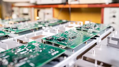
LiDAR boards carry laser drivers, photodetectors, and high-speed processors that tolerate little process variation. Placement accuracy and reflow profile control decide whether those parts sit where the optical design expects. Solder volume must be consistent, because a void under a thermal pad raises junction temperature. Paste inspection before reflow catches volume problems while they are still cheap to correct. Good SMT PCB assembly practice is the foundation here.
Optical components often need alignment beyond standard placement tolerance. Some designs use active alignment, where the part is positioned while a signal is measured. That step requires a defined fixture and a recorded result for each unit. Others rely on mechanical datums and accept the tolerance the housing provides. Either way, the assembly drawing must state which approach applies. Ambiguity at this point becomes scrap or rework later.
Cleanliness also matters more than on a typical control board. Flux residue near an optical surface can scatter light or fog under heat. The cleaning method must be compatible with the components and with any coating that follows. Handling rules should limit exposure to particles and moisture. A factory that treats these boards like ordinary assemblies will show it in yield, so ask how the line is set up for optical work.
Signal Integrity and Layout Review
LiDAR moves large amounts of time-sensitive data between detector, processor, and vehicle network. Impedance control, length matching, and reference plane continuity keep that data intact. A split return path under a high-speed pair turns a clean link into a radiator. Crosstalk between transmit and receive sections can raise the noise floor and cut effective range. Layout review should check these paths before fabrication, not after.
Grounding strategy ties the analog front end, the digital section, and the chassis together. A poorly planned ground can couple laser switching noise into the receive chain. Shielding cans and guard traces help, but they work only when the underlying return paths are sound. Power delivery needs low impedance across the band the load draws, including the fast transients from pulse drive. Decoupling placement follows from that analysis.
Engineers should request a design review that covers stackup, routing, and thermal together. Changes at that stage cost little. Changes after tooling cost a great deal. Teams that need early samples can pair the review with rapid PCBA prototyping to validate the design before volume commitment. The prototype teaches more about the layout than any simulation alone.
Test Coverage and Traceability
Functional test confirms that each module works: laser drive, detector readout, timing, data output, and communication with the vehicle bus. In-circuit test catches wrong or missing parts and opens that functional test may not reach. Boundary scan helps where dense packaging limits probe access. Burn-in exposes early failures that a short bench check will miss. The right mix depends on volume and on how much the program can afford per unit.
Optical performance should be verified against agreed limits, not just checked for activity. Range accuracy, point cloud density, and return strength are the numbers the vehicle program cares about. Test fixtures must hold the unit in a repeatable position, or the data means little. Limits and fixture IDs belong in the record. A structured PCBA testing plan keeps these checks consistent from lot to lot.
Traceability closes the loop. The factory should record which program ran, which component lots were used, and what the inspection found. When a field return arrives, that record is the fastest route to a cause. It also proves that a corrective action reached the next batch. Buyers should ask for these records as routine, because documents that are easy to produce on request are usually kept honestly during production.
Supplier Checks Before Release
A supplier should be able to explain how the stackup was chosen and which tests prove it. Ask for the fabrication drawing, the assembly drawing, and the inspection plan as a set. Confirm that the factory has built similar high-speed or optical boards before. Review how it handles engineering questions and whether changes are documented. A clear answer on these points is worth more than a low quote.
Volume plans should be discussed early, since tooling and test fixtures take time to prepare. A partner that supports both pilot and volume runs under one roof reduces transfer risk. That continuity matters when a design revision arrives mid-program. Buyers can review PCB assembly capabilities against the actual build requirements rather than a generic list. The goal is a process that repeats, not one good batch.
The practical takeaway is simple. Fix the architecture and environment first, then the stackup, then the assembly and test plan. Write every limit down and keep the records with the lot. A LiDAR board that meets its numbers in the lab but cannot repeat them in production is not ready for a vehicle program. Verify repeatability before committing to volume, and the rest of the program gets easier.