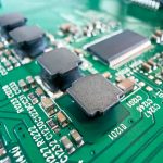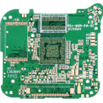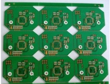
During PCB Manufacturing and PCB prototyping, copper adhesion problems can occasionally occur. One common defect is PCB Copper Peeling, in which a copper trace or copper foil separates from the underlying substrate.
Copper peeling can affect electrical continuity, mechanical reliability, soldering performance, and the service life of the finished PCB. The root cause may originate from circuit fabrication, lamination, copper foil quality, resin compatibility, surface treatment, or PCB design.
Understanding the relationship between copper foil, resin systems, reinforcement materials, and manufacturing processes is therefore essential for improving PCB reliability.
This article explains the major causes of PCB copper peeling and introduces common PCB Substrate classifications.
What Is PCB Copper Peeling?
PCB Copper Peeling refers to the separation of copper foil or a copper circuit trace from the dielectric substrate.
The copper layer is normally bonded to the substrate through a combination of mechanical adhesion, chemical interaction, and resin bonding. If the bonding interface is damaged or the copper is excessively reduced during processing, the conductor may become vulnerable to peeling.
The defect may appear as:
- Local copper lifting
- Partial trace separation
- Copper trace peeling
- Large-area copper delamination
- Copper separation after mechanical stress
- Copper peeling after soldering or thermal cycling
The appearance and location of the defect can provide useful information for determining its root cause.
1. Copper Etching and Circuit Fabrication
One possible cause of copper trace peeling is excessive or uncontrolled etching during circuit fabrication.
During PCB production, copper is selectively removed to form the required circuit pattern. If the etching process is excessive, the conductor may become narrower than the designed width.
This can reduce the mechanical robustness of fine traces and make them more susceptible to external mechanical stress.
Important process variables include:
- Etchant concentration
- Etching temperature
- Spray pressure
- Conveyor speed
- Copper thickness
- Etch compensation
- Circuit density
- Equipment condition
The risk is particularly important for fine-line and heavy-copper designs because the acceptable process window can become narrower.
However, excessive etching should not automatically be identified as the cause of every copper-peeling defect. Failure analysis should also examine the copper-to-substrate adhesion strength and the condition of the interface.
2. Mechanical Damage During PCB Processing
Mechanical impact is another potential cause of copper trace separation.
During PCB Manufacturing, panels may be exposed to mechanical handling, brushing, drilling, routing, transportation, or other processing operations.
If excessive force is applied to a weak copper-to-substrate interface, a trace can partially separate from the substrate.
Typical signs may include:
- Localized copper deformation
- Scratches near the damaged area
- Copper lifted in the direction of mechanical contact
- Visible mechanical marks
- Deformation concentrated around a specific location
If the peeling is caused by mechanical damage, the surrounding copper may still have normal adhesion strength.
Therefore, visual inspection should be combined with adhesion or cross-sectional analysis when necessary.
3. PCB Design and Trace Width
PCB Design can also influence the mechanical robustness of copper traces.
For example, heavy-copper boards may use relatively narrow traces in some areas because of routing requirements. If the conductor width is too small for the electrical and mechanical requirements, the circuit may become more vulnerable to over-etching and mechanical damage.
Designers should therefore consider:
- Copper thickness
- Minimum trace width
- Current capacity
- Etching compensation
- Pad and trace geometry
- Mechanical stress
- Manufacturing tolerances
A design that is technically manufacturable may still require additional process margin if it combines very thick copper with fine traces.
4. Lamination-Related Causes
PCB Lamination is a critical process for establishing reliable bonding between copper foil and dielectric materials in multilayer PCBs.
During lamination, heat and pressure are applied to the multilayer stackup so that the resin flows, fills appropriate spaces, and cures to form a consolidated structure.
If lamination conditions are not properly controlled, the copper-to-substrate interface may have insufficient bonding strength.
Potential causes include:
- Inadequate lamination temperature
- Incorrect pressure profile
- Insufficient resin flow
- Contamination
- Damaged copper foil
- Improper prepreg selection
- Inappropriate lamination cycle
- Incompatible material combinations
In a properly controlled lamination process, the copper foil and resin system should form a stable and reliable interface.
5. Contamination During Lamination
Contamination between copper foil and prepreg can significantly reduce bonding quality.
Possible contaminants include:
- Dust
- Oil
- Foreign particles
- Processing residues
- Oxidation products
- Improperly cleaned surfaces
Because the copper-resin interface is critical to multilayer construction, even localized contamination can create weak bonding areas.
This may result in isolated copper peeling or larger delamination-related defects after thermal or mechanical stress.
Strict cleanliness control during layup and lamination is therefore essential.
6. Copper Foil Quality
The quality of the Copper Foil is another important factor affecting copper adhesion.
PCB copper foil commonly includes electrodeposited copper foil and rolled copper foil, depending on the application.
Copper foil used in PCB fabrication generally has a specially treated surface to improve bonding with the resin system.
The treatment may involve controlled surface roughness and other chemical or electrochemical treatments designed to improve adhesion.
If the copper foil has insufficient bonding performance, the finished PCB may exhibit poor peel strength even when the PCB fabrication process itself is properly controlled.
Important copper-foil characteristics include:
- Copper thickness
- Surface roughness
- Treatment-layer quality
- Peel strength
- Tensile strength
- Elongation
- Surface cleanliness
For high-reliability applications, copper foil selection should be matched to the PCB material and manufacturing process.
7. Compatibility Between Copper Foil and Resin
The compatibility between copper foil and the resin system is particularly important for advanced PCB Materials.
Different laminate systems use different resin chemistries and reinforcement structures. High-Tg, low-loss, lead-free-compatible, and other specialized materials may require copper foil treatments specifically designed for their resin systems.
If the copper foil treatment and resin chemistry are poorly matched, the resulting interface may have insufficient adhesion.
This can become more apparent after:
- Reflow soldering
- Thermal cycling
- Thermal shock
- Mechanical stress
- Repeated soldering
- Long-term operation
Therefore, material compatibility should be evaluated during the material-selection stage rather than after a peeling defect appears.
8. Effect of Copper Foil Surface Roughness
Copper foil surface morphology contributes to mechanical bonding between copper and resin.
A controlled roughened surface can provide additional contact area and improve adhesion.
However, higher roughness does not automatically mean better overall PCB performance.
Excessive roughness may increase conductor loss in high-frequency applications because high-frequency current tends to concentrate near the conductor surface.
Therefore, modern PCB materials require a balance between:
Copper Adhesion + Signal Loss + Surface Roughness + Reliability
This is especially important for high-frequency and high-speed PCB applications.
9. Types of PCB Substrate Materials
The PCB Substrate is the fundamental structural material used to support copper circuits and provide electrical insulation between conductive layers.
A typical PCB substrate consists of:
- Resin
- Reinforcement material
- Copper foil
Different combinations of these materials produce different PCB laminate systems with different mechanical, thermal, electrical, and manufacturing characteristics.
10. Classification by Reinforcement Material
Paper-Based Substrates
Paper-based materials are commonly used in lower-cost PCB applications.
Examples include:
- FR-1
- FR-2
- FR-3
They generally provide lower cost but are not suitable for applications requiring the performance of advanced multilayer or high-frequency materials.
Glass-Fiber-Reinforced Substrates
Glass-fiber-reinforced epoxy materials are widely used in modern PCB production.
Common examples include:
- FR-4
- FR-5
FR-4 is one of the most widely used PCB substrate systems because it provides a practical balance of electrical insulation, mechanical strength, thermal performance, and cost.
Higher-performance materials may be selected when higher Tg or improved thermal reliability is required.
Composite Substrates
Composite materials combine different reinforcement structures or resin systems.
Common examples include:
- CEM-1
- CEM-3
These materials can provide different cost and performance combinations depending on the application.
HDI Build-Up Materials
HDI PCB structures commonly use build-up dielectric materials designed to support microvia formation and high-density interconnection.
Build-up materials may include resin-coated copper (RCC) and other specialized dielectric systems.
Their selection depends on:
- Laser-drilling requirements
- Layer structure
- Resin flow
- Dk/Df requirements
- Thermal reliability
- Fine-line capability
- Via structure
11. Special PCB Substrates
Specialized PCB Materials are available for applications with specific thermal, electrical, mechanical, or environmental requirements.
Examples include:
Metal-Core Substrates
Metal-core PCBs are designed to improve heat dissipation.
Common applications include:
- LED lighting
- Power electronics
- Motor control
- Automotive electronics
Ceramic Substrates
Ceramic materials provide excellent thermal performance and stable electrical characteristics for specialized applications.
They may be used in:
- Power modules
- RF systems
- High-temperature electronics
- High-reliability applications
High-Frequency Materials
High-frequency PCB materials are designed to provide controlled dielectric properties and low signal loss.
They are used in applications such as:
- RF communication
- Radar
- Antenna systems
- Automotive radar
- High-speed networking
12. Classification by Flame Retardancy
PCB laminate materials can also be classified according to their flame-retardant performance.
Common UL94 classifications include:
- UL94 V-0
- UL94 V-1
- UL94 V-2
- UL94 HB
The required rating depends on the product application and applicable safety requirements.
The flame-retardant classification should therefore be selected according to the relevant product standard rather than treated as an independent PCB quality indicator.
13. Classification by Resin System
Another important method of classifying the PCB Substrate is by resin chemistry.
Common resin systems include:
Phenolic Resin
Phenolic resin materials are generally used in cost-sensitive PCB applications.
Epoxy Resin
Epoxy-based laminates are widely used because of their balanced electrical, mechanical, and thermal properties.
FR-4 is a major example of an epoxy-based PCB laminate system.
Polyester Resin
Polyester-based materials are used in selected applications where their specific processing and performance characteristics are appropriate.
BT Resin
BT resin materials provide high thermal performance and are commonly used in advanced packages and high-density interconnection applications.
Polyimide Resin
Polyimide materials provide excellent thermal stability and flexibility and are widely used in flexible and high-temperature PCB applications.
14. How to Prevent PCB Copper Peeling
Preventing PCB Copper Peeling requires control throughout the complete manufacturing chain.
Key measures include:
1. Select suitable copper foil.
Ensure that copper foil peel strength and surface treatment are compatible with the selected resin system.
2. Control PCB design.
Maintain appropriate trace widths and copper geometry, particularly for thick-copper designs.
3. Maintain clean interfaces.
Prevent contamination during inner-layer preparation, layup, and lamination.
4. Optimize lamination parameters.
Control temperature, pressure, heating rate, resin flow, and curing conditions.
5. Control etching.
Prevent excessive conductor loss and maintain the designed trace geometry.
6. Verify material compatibility.
Confirm that the copper foil, prepreg, and laminate resin system are compatible.
7. Perform reliability testing.
For critical applications, use peel-strength testing, thermal stress testing, cross-sectional inspection, and other appropriate verification methods.
15. Failure Analysis of Copper Peeling
When copper peeling occurs, simply replacing the PCB batch may not identify the root cause.
A systematic failure analysis should determine whether the defect originated from:
- Copper foil
- Copper surface treatment
- Lamination
- Resin system
- Etching
- Mechanical processing
- PCB design
- Thermal stress
- Assembly processes
Cross-sectional analysis can be particularly useful because it allows engineers to examine the copper-resin interface directly.
Peel-strength testing can also help distinguish between a general adhesion problem and localized mechanical damage.
Kingda’s Approach to PCB Materials and Copper Adhesion
At Kingda, material selection and process control are considered important factors in preventing PCB Copper Peeling.
Engineering evaluation can include copper foil selection, resin and prepreg compatibility, lamination parameters, copper thickness, circuit geometry, etching control, and reliability verification.
For multilayer and high-density PCB projects, material selection is evaluated together with the required electrical, thermal, mechanical, and manufacturing characteristics.
This integrated approach helps reduce interface-related defects and supports consistent PCB quality throughout production.
Conclusion
PCB Copper Peeling can originate from several different factors, including excessive etching, mechanical damage, inadequate PCB Lamination, copper foil quality, contamination, material incompatibility, and inappropriate PCB Design.
Because the appearance of a copper-peeling defect does not always reveal its true cause, failure analysis should consider both the copper-to-substrate interface and the manufacturing history.
At the same time, selecting the right PCB Substrate is essential for achieving the required electrical, thermal, mechanical, and reliability performance.
Common substrate categories include FR-1, FR-2, FR-3, FR-4, FR-5, CEM materials, HDI build-up materials, metal-core substrates, ceramic substrates, and specialized resin systems such as BT and polyimide.
By combining appropriate PCB Materials, controlled lamination, accurate circuit fabrication, reliable copper foil, and effective quality control, manufacturers can significantly reduce the risk of copper peeling and improve overall PCB reliability.