Custom Shape PCB Milling Service: Tolerance, Capacity and Cost
What Profile Milling Is
Profile milling, also called routing or outline machining, is the step that turns a panel of circuits into individual boards of the required shape. A high speed spindle follows the outline from the mechanical layer of the design data and cuts the profile with a small diameter cutter, which means the finished board can be round, elliptical, curved, polygonal or completely irregular. A rectangular outline is the trivial case; the reason the process matters is that a great many modern products cannot use a rectangle, and the shape has to be produced after all the plating, masking and finishing steps are complete without damaging anything that has already been built.
The Milling Sequence
Data review. The fabricator imports the Gerber set, the drill file and the outline data, and the CAM engineer confirms that the profile is closed, that the copper sits inside it with the required clearance and that any internal cutout can be reached with an available tool.
Path generation. The outline is converted into a tool path, with the cutter diameter compensated so that the finished edge lands on the drawn contour rather than on the centre line of the tool.
Tool selection. Cutters are commonly stocked at 0.8 mm, 1.0 mm, 1.6 mm and 2.0 mm. A smaller tool follows a tighter radius but cuts more slowly and wears faster, so the choice is a trade between geometry and throughput.
Routing. The spindle cuts the profile at high rotational speed, often in several passes, with tabs left in place so that the boards stay attached to the panel through the remaining handling and test steps.
Depanelisation and finishing. The tabs are cut, the edge is deburred, and the board is cleaned and inspected. For shaped boards with fine features near the edge, this is the step where damage usually occurs if the tooling or the handling is careless.
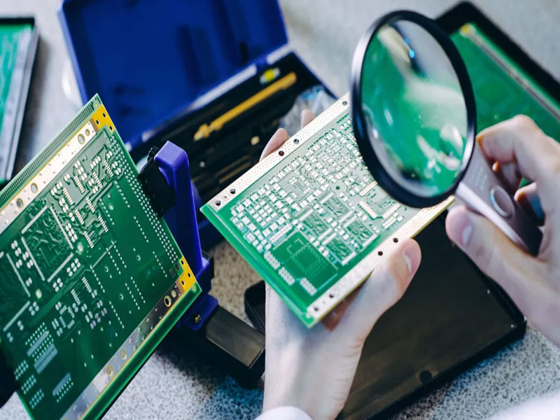
Dimensional check. The outline is measured against the drawing, either with a vision system or with a gauge, because the profile is a mechanical interface and a board that misses the tolerance may not fit the enclosure at all.
Why Shaped Boards Are Everywhere Now
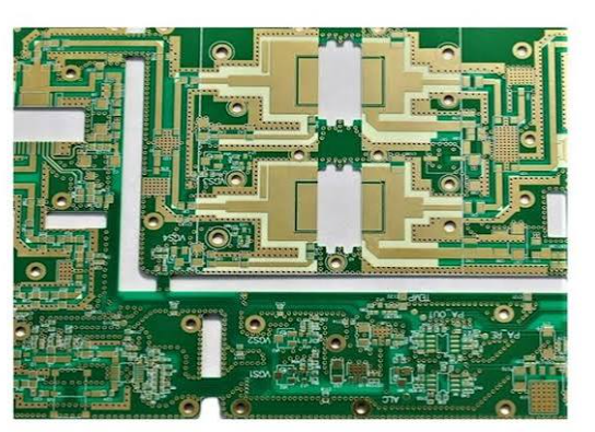
Space is the usual answer. A wearable, a hearing aid, a sensor module or a camera assembly often has a curved or irregular housing, and a rectangular board wastes the space at the corners that the product cannot afford to lose. A round board for a round housing also removes the need for a mounting bracket, which saves cost and assembly time. In some products the shape is functional: an antenna array or a matching structure may need a specific outline, a potted assembly may need the board to match a cavity, and a rigid flex design may need a curved section that a rectangle cannot provide. Aesthetics matter too, particularly in consumer products where the board may be visible, and there are applications such as LED rings and instrument dials where the shape is the product.
What a Milling Service Can Hold
The practical capability limits are set by the smallest cutter available, the board thickness and the accuracy of the router. Internal cutouts and slots cannot be narrower than the tool, so a 0.8 mm cutter sets roughly a 0.8 mm minimum slot width, and corner radii inside a cutout cannot be smaller than the tool radius. Thicker boards and heavy copper loads increase the cutting force and push the tool towards a larger diameter and a slower feed. Depth control matters where the profile is only partly cut, as in a stepped edge or a counterbore, and that capability should be confirmed rather than assumed. The outline tolerance itself is normally held within about plus or minus 0.1 to 0.2 mm for a routed profile, with tighter values available on a dedicated process at higher cost.
Design Rules That Keep the Profile Buildable
Give the outline as a single closed contour on its own layer, with arcs rather than approximated curves. Keep the corner radius at least as large as the radius of the cutting tool, so that the intended shape is achievable without leaving a rounded corner where a sharp one was drawn. Keep copper and any critical features away from the edge, typically 0.3 to 0.5 mm for a routed edge, because the cutting process has a tolerance and a burr that can reach further than the nominal contour. Define the tabs deliberately: place them in areas with no components and no fine traces, keep them wide enough to support the board through assembly and specify how they will be removed. Where the board has to fit a mechanical part, put the tolerance and the datum in the drawing, and check the internal cutouts against the tallest component that has to pass through them. If the shape includes a bend line on a flex section, keep the outline data consistent with the flex layer so the CAM engineer is not reconciling two different interpretations.
Profile Milling Compared With Other Separating Methods
V-cut scoring is fast and cheap for straight lines on rectangular panels of uniform thickness, and it leaves a clean edge with a small chamfer, but it cannot produce a curve or an internal cutout. Stamp hole, or breakaway tab with drilled perforations, suits small boards and dense panels where the components are close to the edge, and it leaves a rougher edge that usually needs cleaning. Laser cutting produces very fine features and can cut hardened or unusual materials, but the edge is often charred or tapered and the method is expensive at volume. Profile milling is the most flexible of the four: it handles any shape, any internal cutout and any panel format, at the cost of a slower cycle and a tool that wears. On a shaped board there is rarely a real alternative.
What Drives the Price
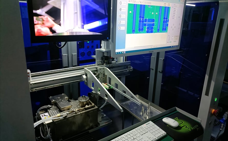
Milling cost is dominated by machine time and by the number of separate operations the panel requires. A long perimeter takes longer to cut than a short one, a tight radius forces a slower feed with a smaller tool, and a thick board or heavy copper slows the process further. Internal cutouts and stepped edges add path length and often a second setup. Low volume orders carry the programming and tooling setup across fewer boards, which is why the per piece price of a shaped prototype board looks high compared with a rectangular one, and why the gap narrows as the quantity rises. Panel design matters as well: a layout that leaves adequate room between boards allows a larger cutter and a faster pass, while a tight panel forces a small tool and more passes. Where the shape permits, enlarging the corner radius and widening the slots is one of the cheapest ways to reduce the price.
Cutting the Cost Without Cutting Quality
Use the largest radius the product allows, since it lets the fabricator choose a larger and faster tool. Avoid decorative detail that serves no mechanical purpose, because every extra contour is machine time. Group the cutouts so they can be reached in a single setup. Keep the panelisation sensible, with enough material between boards for the cutter and for the tabs. Confirm the outline tolerance that actually matters for the fitting, and do not specify a tighter one out of habit. Finally, send the outline as a clean closed DXF along with the Gerber data, since profile repair at the CAM stage is engineering time that shows up on the invoice.
FAQ
What is the smallest slot that can be milled? Roughly the diameter of the smallest cutter available, commonly 0.8 mm, and a slot narrower than that has to be produced by another method or widened in the design.
Can a rounded corner be avoided? Only by using a smaller tool, and there is still a minimum radius. Draw the radius the product actually needs, since a sharp interior corner cannot be routed.
What tolerance can be held on the outline? About plus or minus 0.1 to 0.2 mm is typical for a routed profile, with tighter control available at additional cost and longer lead time.
Should I use milling or V-cut for a rectangular board? V-cut is faster and cheaper when every board is rectangular and the panel has straight parallel lines. Milling is better when the outline is irregular or the components sit close to the edge.
Does the shape affect the copper clearance rules? Yes. Keep copper and fine traces 0.3 to 0.5 mm inside the outline so that the routing tolerance and any burr do not reach the circuitry.
Conclusion
Profile milling is what allows a board to be a mechanical part rather than a rectangle, and it works best when the outline is designed for the process: closed contours, sensible corner radii, clear tabs and enough clearance between the copper and the edge. Confirm the tooling limits with the fabricator before finalising the shape, send a clean DXF so that the CAM engineer is not guessing, and define the outline tolerance that the assembly actually needs. The shaped board capability of a supplier is normally listed alongside its standard limits in PCB capabilities, the mechanical conventions belong in PCB design and layout, and the routing and inspection steps that follow are described in PCB manufacturing. A prototype PCB assembly build is the quickest way to prove the shape fits before volume production in 2026.