Industrial Data Acquisition Board Design: Pitfalls and Fixes
An industrial data acquisition board is judged by measurement quality rather than by feature count. A design that samples quickly and offers many channels but cannot hold an accurate reading in a noisy plant environment has solved the wrong problem. Most of the difficulty is not in the converter or the software, but in the analogue front end, the grounding strategy and the way the board handles the hostile electrical environment around it.
Where Measurement Accuracy Is Lost
Accuracy is lost in small increments along the whole signal chain. A reference that drifts, a front end whose input impedance loads the sensor, a ground difference between the signal source and the converter, and digital noise coupling into the analogue path each contribute a share. Recovering them requires understanding which mechanism dominates at the resolution the design targets.
The starting point is a noise budget: how many bits of resolution the design claims, what that means in microvolts, and how the available error sources compare against it. A sixteen bit converter at a five volt range is working at roughly seventy six microvolts per code, which is a useful reminder of how small the disturbances have to be before they matter.
The Analogue Front End and Its Reference
The front end sets the relationship between the sensor and the converter. Series resistance, input filtering and any amplification all have to be chosen together, because a filter that is too aggressive slows the response while one that is too permissive admits noise. Where the sensor is remote, the cable and its capacitance become part of the circuit and cannot be ignored.
The reference deserves the same attention. Its noise and temperature coefficient appear directly in the measurement, and any current flowing in the reference path modulates the reading. A reference decoupled with a capacitor placed close to the pin, connected to the analogue ground rather than the digital one, is a small detail with a large effect. Our notes on power plane splitting rules explain how supplies are separated when the analogue and digital domains share a board.
Grounding Strategy Across the Isolation Barrier
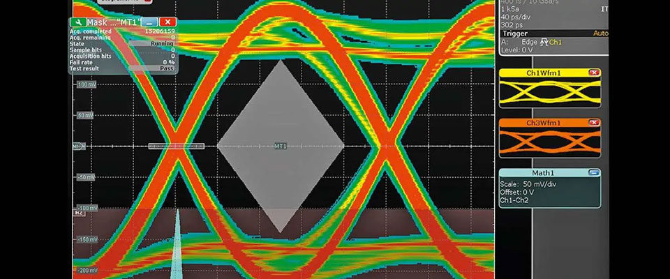
Industrial inputs are frequently isolated, and the isolation barrier is where grounding decisions become critical. On the field side, the reference is the sensor ground, which may sit at a different potential from the control side. On the logic side, the reference is the system ground. The two meet only through the isolation device, and the layout has to ensure that no other path connects them.
A single inadvertent bridge, such as a mounting hole connected to both grounds or a shield tied to the wrong side, defeats the isolation and allows the difference in potential to drive current through the board. Keeping the boundary explicit on the layout, with a clear keepout band and no copper crossing it except the isolation component itself, is the practical way to protect the design.
Noise Sources: Switching Supplies and Digital Return
Switch mode supplies are efficient and noisy, and their noise appears as conducted and radiated interference across the board. The switching loop should be kept as small as possible, the inductor and the output capacitor placed together, and the ground return for the converter kept separate from the analogue ground until a defined single point.
Digital return currents are the second source. A microcontroller bus switching at tens of megahertz produces a voltage gradient across the ground plane, which appears at the analogue input as noise even though no trace connects the two circuits. Our notes on EMI suppression design principles describe how loop area and reference continuity govern that coupling.

Channel to Channel Crosstalk in Multiplexed Systems
Multiplexed inputs share an analogue path, which means a high level signal on one channel can leave charge on the sampling capacitor that affects the next channel read. The error appears as a small offset that depends on the previous reading, and it is easy to mistake for noise.
Mitigation is partly architectural, since the converter and the multiplexer determine how much charge transfer occurs, and partly a layout matter. Keeping the analogue input traces short and evenly matched, avoiding long stubs to unused channels and placing the input filters as close to the connector as possible all reduce the effect. Where a channel is unused, terminating it properly is better than leaving a floating node that can couple into the active measurement.
Calibration, Test Points and Production Trim
An accurate board is usually a calibrated board. Providing a means of applying a known reference during production test, and of measuring the front end at that reference, allows the gain and offset to be corrected. That facility has to exist in the layout, which means test points or a calibration connector rather than a procedure that relies on probing fine pitch pads by hand.
Temperature drift is usually handled by a combination of component choice and software calibration across temperature. Where the drift is measured, the measurement path itself has to be stable, which brings the design back to the reference, the front end and the grounding strategy.
Layout Checks Before Release
Before the board is released, check the things that are expensive to change later. Confirm that the isolation boundary is unbroken, that the analogue and digital grounds meet at exactly one point, that the reference is decoupled with a short return path, and that the switching supply loops are as small as the layout allows.
Then check the mechanical and service aspects: connector retention, access for calibration, and the routing of any cable that carries low level signals near a switching supply. Our outline of layout verification methods places those checks before fabrication, where a correction costs an afternoon rather than a production run.
Enclosure, Wiring and the Wider Installation
The board does not exist in isolation, and a large share of field problems come from how it is installed. Cable shields connected at both ends create ground loops that inject current through the signal return, while shields connected at neither end achieve nothing useful. The enclosure ground, the sensor ground and the system ground have to be considered together, and the board design should make the intended connection scheme obvious rather than leaving it to the installer to guess.
Documenting that scheme on the drawing, and providing the terminals or pads that make it easy to follow, is part of the electrical design. Where the installation depends on a wiring convention, state it explicitly and verify it during commissioning.
FAQ
Should the analogue and digital grounds be joined or kept apart? Joined, at one defined point, with the analogue and digital regions each having their own copper area. Fully separate grounds create a potential difference that becomes a noise source, while a single connection gives both regions a reference without letting digital return currents flow through the analogue area.
How important is the reference for a data acquisition board? It is usually the limiting factor on absolute accuracy. Reference noise and temperature drift enter the measurement directly, and any current flowing through the reference connection adds an error proportional to the impedance of that path. Treat the reference as a signal, not as a supply.
Does isolation remove the need for careful grounding? No. Isolation removes the galvanic connection between the field side and the logic side, but the layout must ensure that no other path reconnects them. Grounding within each side still matters, and a bridge across the barrier is one of the most common ways an isolated design loses its isolation.