Direct Bonded Copper PCB: Structure, Materials and Process
Power electronics has been pushing against the limits of ordinary boards for two decades. An insulated gate bipolar transistor module that switches several hundred amps produces heat in a volume smaller than a fingernail, and no laminate with an organic dielectric can move that heat away fast enough. Direct bonded copper solves the problem by removing the organic dielectric altogether and bonding copper straight to ceramic.
The Structure of a Direct Bonded Copper Board
The construction is simple to describe and difficult to make. A ceramic sheet carries a layer of copper on one or both faces, typically three hundred to eight hundred micrometres thick, which is then etched into the circuit pattern. There is no adhesive and no resin between the metal and the ceramic.
That absence of an interlayer is the whole point. An organic dielectric under a power device contributes most of the thermal resistance in the stack, so deleting it takes the junction temperature down and lets the same die run at a higher current. The ceramic also provides the isolation between the top pattern and the baseplate.
How the Bond Is Formed
The bond relies on a eutectic reaction between copper and oxygen. The copper foil is oxidised to a controlled and very thin surface layer, brought into contact with the ceramic, and heated to roughly one thousand and sixty five degrees Celsius in a nitrogen atmosphere. At that temperature a copper oxygen eutectic liquid forms at the interface and wets the ceramic.
On cooling, the liquid solidifies and leaves a continuous bond with no organic residue. The process window is narrow, because too little oxide gives a weak bond and too much leaves voids, and the furnace atmosphere has to stay within a tight oxygen range. That sensitivity is why the process is concentrated in a small number of specialist plants.
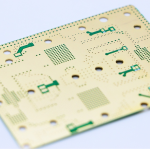
<img src="https://www.gopcba.com/wp-content/uploads/2026/08/262.webp" alt="Direct bonded copper PCB with thick copper pattern” />
Ceramic Selection
Alumina is the traditional choice for a direct bonded copper ceramic substrate. Its conductivity is around twenty four watts per metre per kelvin, which is modest, but it is cheap, well understood and available in large sheets, so it suits converters and motor drives that do not run at the highest power density.
Aluminium nitride raises the conductivity to roughly one hundred and seventy watts per metre per kelvin and matches the expansion of silicon closely, which makes it the choice for high performance modules. Silicon nitride is a third option with a lower conductivity around ninety but markedly better mechanical toughness, and it is preferred where the module has to survive severe thermal cycling or vibration.
Copper Thickness and Current
Thick copper is what allows the pattern itself to carry the load current and to spread heat sideways under the die. A three hundred micrometre foil suits medium power devices, five hundred micrometres is common in high current designs, and eight hundred micrometres or more appears in the largest modules.
The penalty is etch behaviour. A thick foil undercuts significantly during etching, so the minimum gap between conductors grows with thickness, and the designer has to accept wider tracks and larger spacing than on a conventional board. Sizing those conductors still follows the same principles as any other copper, described in trace width and current calculation.
Patterning and Etching
The copper is patterned after bonding, by photolithography and chemical etching, or in some cases by laser cutting for simple outlines. Etch compensation has to allow for the sideways attack on a thick foil, and the profile of the sidewall matters because a wedge shaped track has a smaller cross section than its top width suggests.
Inspection after etching is done by microsection on a sample, because the sidewall profile cannot be judged optically through the resist. The measurement that matters is the width at the base of the track rather than at the top, since that is the metal that actually carries the current, and a supplier who reports only the top width is not giving a usable figure.
Where a fine pattern is needed alongside a thick power pattern, some designs mix processes and use a plated layer for the control circuit on the same substrate. That is a compromise rather than a standard route, and the fabrication sequence has to be agreed with the supplier before the layout is drawn.

Thermal Cycling and Reliability
Temperature cycling is the accepted measure of a direct bonded copper board, and it is normally run between minus forty and one hundred and twenty five degrees Celsius or over a wider range for automotive qualification. The failure mode is a crack that starts at the copper edge and propagates through the ceramic.
Copper thickness, ceramic type and pattern geometry all influence the result. Thin copper and silicon nitride give the longest life, which is why they appear together in traction modules, while a thick copper pattern on alumina has the shortest. The die attach follows the same rules, which is where the alloy discussion in lead-free versus leaded solder becomes relevant.
Design Rules for Power Modules
Round every internal corner of the copper pattern, since a sharp corner concentrates the stress that drives the crack. Keep the copper well inside the ceramic edge, because the unsupported ceramic at the periphery is the weakest region. Where copper appears on both faces, balance the areas so that the part does not bow during cooling.
Plan the thermal path before the electrical layout. The die position sets where the heat enters the substrate, the copper under it spreads that heat, and the baseplate removes it. A converter built around that sequence behaves predictably, and the layout considerations in DC-DC converter layout and routing apply to the control side of the same board.
Cost and Sourcing
Cost tracks ceramic material, copper thickness and substrate area. Alumina with three hundred micrometre copper is the affordable end of the range, aluminium nitride with eight hundred micrometres is several times more, and yield falls as area grows because a single defect spoils a large part.
Sourcing options are limited, so the practical question is not only price but process stability. Ask for cycling data, copper peel strength and dimensional tolerance together, and treat a supplier who can provide all three consistently as more valuable than one who quotes a lower unit price with no evidence behind it. Lead time follows the same logic, since a bonded substrate cannot be expedited once the furnace schedule is set, and a programme that plans for the process rather than against it avoids most of its schedule risk.
FAQ
Is a direct bonded copper board the same as a metal core board? No. A metal core board has an organic dielectric between the copper and the aluminium base, while a direct bonded copper board bonds copper to ceramic with no organic interlayer at all.
Can components be soldered onto it? Yes. The etched copper is solderable, and surface mount devices, shunts and connectors are attached with conventional reflow or with sintering for the power die.
How does it compare with a plated ceramic substrate? Plated processes give finer lines but thinner copper, so they suit control circuits and fine pitch parts. Direct bonding wins wherever current and thermal cycling dominate.