Embedded Chip PCB: Putting Power Devices Inside the Board
An embedded chip PCB reverses the usual relationship between a component and its carrier. In a half year report published in August 2026, a Chinese board manufacturer described a technology that embeds power dies directly inside the printed circuit rather than mounting them on the surface, reporting parasitic inductance reduced by more than ninety percent, power density improved two to three times, product area reduced by thirty to fifty percent, and a projected cost reduction of twenty to thirty percent at volume.
The applications named were AI server power supplies and robot joint drives, where the company reported that joint volume could shrink by sixty to eighty percent with response speed improved by more than half and power cycling capability above one hundred thousand cycles. Those figures describe a change in what a board is for: from a platform that connects devices to a structure that contains them.
What Chip in Board Changes
A conventional power module stacks a die, a package, a substrate, terminals and a board, and each layer adds length to the current path. Embedding the die inside the board removes several of those transitions and shortens the loop between the device and the copper that connects it.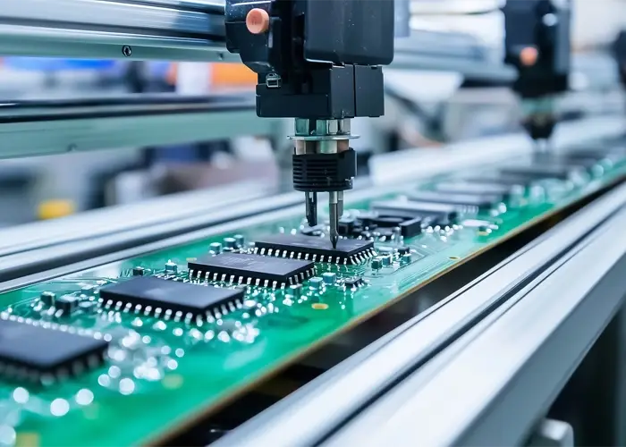
The change is architectural rather than incremental. Once the die is inside the board, the copper layers become part of the package, the dielectric becomes part of the insulation system, and thermal management becomes a property of the laminate construction. Design authority shifts from the package engineer to the board engineer.
Why Parasitic Inductance Matters So Much
When a power device switches, current changes quickly and the inductance in its loop converts that change into a voltage spike. Reducing loop inductance reduces the spike, which allows faster switching with the same voltage margin or the same switching speed with a smaller margin and less loss.
A reduction of ninety percent is significant because gate and power loops are the parts of the circuit that designers cannot fix in software. Every millimetre removed from the loop is a real improvement in efficiency and in electromagnetic behaviour, and it is the primary technical argument for embedding rather than improving a conventional module.
Power Density and Area
Embedding also removes the vertical space occupied by packages and their interconnections, which allows the same function in a smaller footprint, or more function in the same footprint. Reported area reductions of thirty to fifty percent follow from that geometry rather than from a new semiconductor device.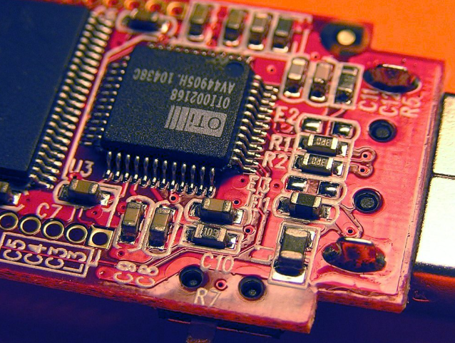
For a robot joint this matters disproportionately, because the electronics must fit inside a mechanism whose volume is set by the motor and gearbox. Reducing board area and height changes what the mechanical designer can achieve, which is why embedded power technology appears first in applications where space is the limiting resource.
Thermal Paths Inside the Board
Heat from an embedded die must travel through the surrounding laminate and copper to reach a heatsink or the enclosure. Copper planes below and above the die act as spreaders, and thermal vias carry heat through the stack, but the laminate itself has lower conductivity than a ceramic substrate.
Design therefore concentrates on creating a low resistance vertical path directly beneath the die and on keeping other heat sources away from it. Thick copper, filled vias and, where the design allows, metal cores or inserted thermally conductive materials are used, and the thermal design is verified by measurement because the models depend on material properties that vary with temperature.
How Embedded Dies Are Manufactured
Producing an embedded die board usually begins by placing the die in a cavity or on a carrier, then laminating dielectric around it and building up copper layers on top. The die must survive the lamination temperature and pressure, which constrains the materials that can be used and requires a process developed specifically for the purpose.
Registration is critical because connections to the die pads are made through the build up, and small misalignments reduce yield. Manufacturers developing this technology invest heavily in process control, since a finished board contains an expensive die and a defect discovered late wastes both the die and the work already done. That investment is characteristic of advanced board manufacturing.
Yield and Rework
Rework is the uncomfortable question with embedded components. A surface mounted part that fails can be replaced; a die inside the laminate cannot. Yield therefore has to be high enough that scrapping embedded units remains economical, and testing has to catch defects before the build up is completed wherever possible.
In practice manufacturers test at intermediate stages, use known good die and inspect after each lamination. That discipline is why the technology appears first in products where the value of density and performance justifies the process, rather than in cost sensitive designs where a conventional module remains adequate.
Robot Joint Drives as an Early Application
A robot joint contains a motor, a gearbox, an encoder and a drive, all inside a package sized by the mechanism. The drive board is often the component that forces the joint to grow, and shrinking it changes the whole articulation.
Embedding the power stage reduces the board area and the height, and the shorter loop improves switching behaviour, which helps control quality. Reported figures for volume reduction and response improvement are consistent with that reasoning, and the power cycling capability matters because a joint drive experiences continuous thermal and electrical cycling in service.
Power Supplies for Accelerators
Server power supplies have moved toward higher density as rack power has risen, and a power stage that occupies less area with lower inductance is attractive for the same reasons it is attractive in a robot. The board becomes a module with a defined electrical and thermal interface rather than a platform carrying components.
For data centre deployment, reliability and serviceability remain the deciding factors. A supply built around embedded dies has fewer mechanical interfaces, which can improve reliability, but it also concentrates risk if a unit fails. Designing the system so that a supply can be replaced without disturbing the rest of the rack is part of making the technology practical.
Cost at Volume
The projected twenty to thirty percent cost reduction at volume comes from removing package material, terminals and assembly steps, and from using board processes to do work that packaging processes previously did. At low volume the opposite is true, because process development and tooling dominate.
This makes embedded power a volume technology. It becomes economical where a product ships in large quantities and the design is stable, which is exactly the situation in robot joints and power supplies destined for standardised racks. Programmes still iterating on a design are better served by conventional modules until the requirement settles, then by a transition once volumes justify the manufacturing capability.
Design Rules for Embedded Power
Designers working with embedded dies have less freedom than with surface components. The die position affects copper balance and via placement, thermal paths are fixed early, and the layer arrangement must accommodate both the die cavity and the build up connections. Changes after lamination are impossible.
The practical response is to model the electrical and thermal behaviour before the first build and to keep design margins for the second iteration, because the first embedded design rarely performs exactly as predicted. Working with a manufacturer who has built the structure before is more valuable here than in most applications, and it is the reason the process route should be agreed before the layout is finalised.
Where Embedded Power Fits Best
The technology pays off where three conditions coincide: space is severely limited, switching performance matters, and volumes are high enough to justify process development. Robot joints and server power supplies satisfy all three, which explains why they appear first.
It fits poorly where a design is still changing, where quantities are small, or where a conventional module already meets the requirement at lower total cost. Recognising those cases early avoids investing in a process the product cannot amortise, which is a commercial judgement as much as a technical one.
Working With the Manufacturer
Embedded designs are co-developed rather than specified. The manufacturer has to know the die, the thermal load, the switching frequency and the mechanical envelope before the layout makes sense, and the designer needs to know which structures the process can produce reliably.
That relationship works best when electrical and thermal models are shared early and the first build is treated as a learning step. Programmes that plan for a second iteration generally reach production faster than those expecting the first embedded design to be final, and they spend less time resolving problems after the board is built.
Qualification for Embedded Assemblies
Qualification must cover electrical performance, thermal behaviour under cycling and mechanical integrity of the laminate around the die. Because the die cannot be inspected directly, indirect methods such as thermal imaging under load and electrical parameter measurement are used to detect degradation.
Power cycling tests are the most informative, since they reproduce the conditions that separate a good design from a fragile one. A reported capability above one hundred thousand cycles is a meaningful claim in that context, and it is the kind of evidence a buyer should ask for before committing a product to an embedded construction rather than after the first field returns, which is where quality management proves its value.