PCB EMC Problems: Finding the EMI Source and the Coupling Path
When a product fails an EMC test, the temptation is to reach for the enclosure and the cables first and start wrapping. That approach sometimes works and never explains itself, and it produces a product whose compliance depends on a piece of foil that a later cost reduction may remove. The approach that works is to identify the source, identify the path the energy takes, and then fix the specific mechanism rather than the symptom.
Start with the Source
The first question is which device on the board is generating the energy that reaches the measurement antenna or the line impedance stabilisation network. Without that answer, every later measure is a guess.
The usual board-level EMI source candidates are well known: the crystal or oscillator, the switching regulator, any clock generator or buffer, high-speed data interfaces, and voltage-controlled oscillators in radio sections. Each of them is characterised by a current that changes quickly, and the loop that carries that current is the antenna.
The sources that come from outside the product matter as much, because a product has to work in their presence as well as not emit. Wireless transmitters, motors, contactors, welding equipment and electrostatic discharge events all deliver energy that the product has to tolerate. The immunity case is usually the harder one for a small product with a plastic enclosure, because there is no shielding to begin with.
Energy also moves by conduction rather than by radiation. The coupling path in that case is a conductor: the power cable that brings the disturbance in, the signal cable that carries it out, or a shared ground return through which two circuits exchange noise. The last of these, common impedance coupling, is the one that appears most often on a board and the one that is easiest to overlook, because the two circuits are not connected to each other in the schematic; they only share a conductor.

The Coupling Mediums
Between the source and the outside world there is always a medium, and naming it shortens the investigation.
An unintentional antenna is the first. It can be a trace that is long compared with the wavelength of interest, a cable that acts as a monopole, or a mechanical structure. Reducing the current in the antenna or shortening it reduces the emission directly.
The enclosure is the second. A metal enclosure is a shield if it is closed, and a resonant cavity if it is not: an opening that is a significant fraction of a wavelength radiates efficiently, which is why a slot between two poorly bonded panels, or a row of ventilation holes, can radiate as effectively as an intentional antenna. The rule that follows is that aperture dimensions matter more than total open area.
The shared ground structure is the third medium, and it is the one that couples circuits inside the product. Two currents that use the same conductor see the conductor as a shared impedance, and the voltage that develops across it is the noise that appears at both circuits.
The interconnect and the power cable are the fourth. Both are long, both leave the enclosure, and both carry the currents that a conducted emissions measurement looks for. A cable that is not terminated to the chassis at its entry point has a high impedance path to ground, so the common mode current that develops on it has no way to return inside the product.
Grounding, and What It Is For
The word grounding covers several different jobs, and mixing them up is a source of confusion.
Safety grounding provides a low impedance path from the enclosure to earth so that a fault current trips the protection rather than passing through a person. It is defined by the safety standard and it cannot be traded for an EMC benefit.
The signal reference is the potential against which a circuit measures its inputs. On a board, that is the grounding plane, and its quality is measured by the impedance between the point where the signal returns and the point where the circuit measures. A large loop area raises that impedance and increases both the emission and the susceptibility at the same time.
Grounding is also what makes shielding work, because a shield that is not grounded at multiple points does not carry the induced current that gives it its effect. The same is true of filters: an EMI filter works by diverting the disturbance to ground, and it can only do that if the ground connection at the filter is short and low in impedance. A filter placed at the connector with a long ground path to the chassis behaves like a small capacitor with a large inductor in series, which is to say it barely behaves like a filter at all.
Filtering and Shielding as Measures
Filtering is the primary tool for conducted disturbance. Almost all of it is low-pass work: the wanted signal occupies a band, and the filter has to pass that band while attenuating everything above it. Power line filters and signal line filters are built the same way, with the difference that a signal filter has to be transparent to a much wider band and often has to preserve the characteristic impedance of the line.
Where a filter is used on a differential pair or a high-speed line, its parasitic capacitance and inductance become part of the circuit, and a filter that attenuates the interference may also distort the signal. That is why filtering on a high-speed interface is normally reserved for lines that leave the board, and why those lines are the ones whose return paths deserve the most attention. Where a shielded section is unavoidable, the shield frame and lid are assembled with the rest of the surface mount parts, which is standard work in our SMT assembly process.
Shielding works by reflection and absorption. A conductive enclosure reflects the incident field and carries a current on its surface that produces an opposing field, and the effectiveness depends on the material, the thickness at the frequencies involved, and above all on the continuity of the enclosure. Two panels that are bolted at four corners are not a continuous shield; the seams between them are apertures, and the apertures are what the field uses.
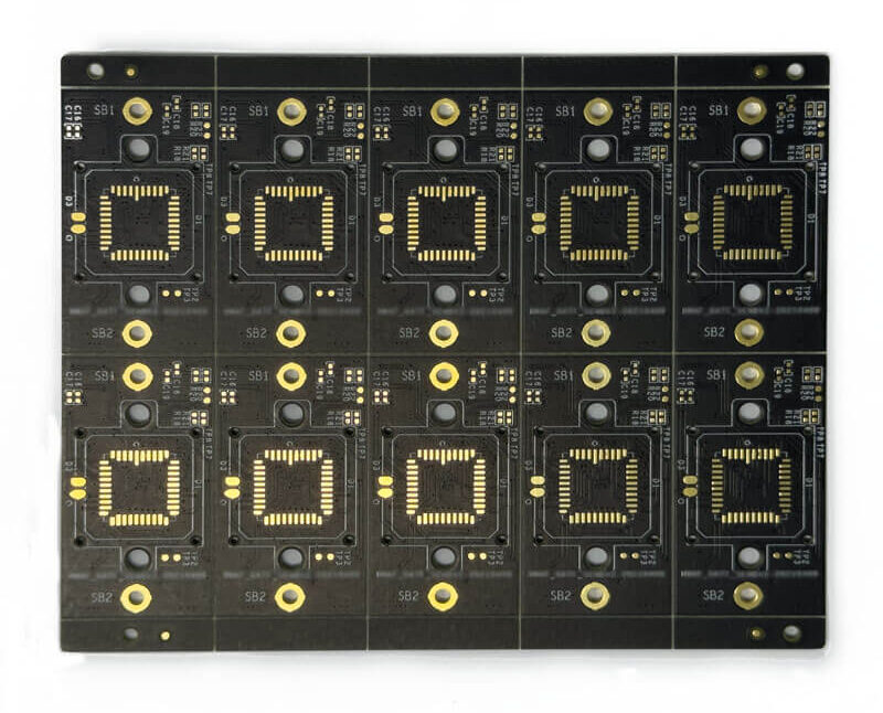
<img src="https://www.gopcba.com/wp-content/uploads/2024/09/PCB-boardsjpg.jpg" alt="common impedance coupling through a shared ground return” />
Simulation and Its Limits
Simulation is useful at the level of the mechanism rather than at the level of the final measurement. A signal integrity analysis can show the overshoot and ringing on a line and can demonstrate the effect of slowing an edge or adding series termination. A power integrity analysis can show the impedance of the plane pair across frequency and show which capacitor placement flattens it. Both of those are real improvements in the mechanism, and both can be verified by comparing the result before and after the change.
What simulation cannot do reliably is predict the final measurement in the chamber, and the reason is the number of factors that contribute. A change that improves one path may have no measurable effect because a different path dominates. A measure applied with the wrong impedance reference can make the situation worse. And measures interact: two filters in series can resonate, and an extra shield can change the current distribution in a way that increases the emission from a seam.
The practical conclusion is that a board should be simulated to make the mechanisms visible and compared before and after a change, rather than being simulated to predict a compliance result.
What Software Can Do
Some disturbance can be handled after the signal has been captured, and it is worth using the available margin rather than leaving it unused. Redundancy and fault tolerance allow a system to ignore a corrupted sample. Error detection through flags and checksums lets the system reject data it cannot trust. Digital filtering removes interference that does not share the characteristics of the wanted signal. A watchdog recovers a system that has been disturbed into an invalid state.
None of these reduce the emission of the product, but they raise its immunity, and they are cheap because they are written rather than built. A design that uses them well may pass an immunity test with a simpler board than one that relies on hardware alone.
Working Order
Identify the source. Name the coupling path. Fix the mechanism: shorten the loop, terminate the cable shield to the chassis, place the filter where it can reference the ground it needs. Only then, and only if the margin requires it, add shielding. Our layout review applies that order to the board, and for products that are certified as a complete unit the construction details that make the measures repeatable are held with the build record in our quality management system.
FAQ
Why did adding a shield not fix the emission? Because the energy was leaving by another path, most often a cable that was not terminated to the chassis, or a seam that the shield introduced.
Is a metal enclosure always a shield? No. It behaves as a resonant cavity if its openings are close to a wavelength in size, and then it can radiate more than an open product would.
Can EMC be fixed in firmware? Immunity can be improved substantially in firmware. Emissions cannot, because they are produced by the physical currents on the board.