




ENIG Surface Finish: Process, Thickness and Performance
Electroless nickel immersion gold is the surface finish that most engineers specify when they want a flat, long lasting, solderable pad and are prepared to pay for it. It is the finish of choice for fine pitch components, for ball grid arrays and for boards that will be stored for months before assembly, and it is also the finish that has caused more process controversy than any other because of the failure mode known as black pad. Understanding the process explains both why it is specified and where it goes wrong.
The Two Layers and What Each Does
ENIG is two coatings applied in sequence. The nickel is deposited by an electroless chemical reaction rather than by electroplating, which means no current path is needed and every exposed copper surface is covered uniformly, including the inside of a hole and the walls of a fine feature. The gold is then applied by immersion displacement, where the gold ions in solution displace nickel atoms on the surface until the nickel is covered and the reaction stops on its own.
The nickel is the functional layer. It provides a hard, solderable surface that resists oxidation and diffusion, and it stops the copper beneath from migrating into the joint. The gold is a protective layer: it prevents the nickel from oxidising during storage and it is thin enough, typically a few hundredths of a micrometre, that it dissolves completely into the solder during reflow. If the gold is too thick, it forms brittle intermetallic compounds in the joint, which is why the thickness is specified as a maximum as well as a minimum.
The Process Sequence
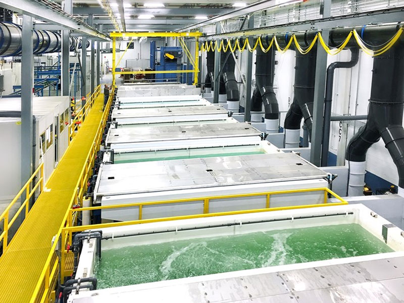
Preparation matters more than any other step. The copper surface must be clean and free of oxide, and it must be suitably rough at the microscopic level for the nickel to adhere. The panel is cleaned, microetched to remove oxide and a small amount of copper, and then catalysed with a palladium-based activator that provides the nucleation sites for the nickel to grow on.
The nickel bath then deposits the metal at a controlled rate to a specified thickness, typically between three and six micrometres. The bath chemistry, its temperature and its pH all affect the deposit, and a bath that is out of specification produces a nickel layer with high phosphorus content and poor solderability. Gold follows, and then a rinse and dry. Between each step the panel is rinsed thoroughly, because drag-in of one chemistry into the next is a common cause of defects. Our design release checklist covers the items to confirm on the finish specification.
Black Pad and How It Happens
Black pad is the failure that made ENIG controversial. It appears as a dark, brittle layer at the interface between the nickel and the copper, and a joint made over it fractures with little mechanical strength even though it looked sound. The cause is corrosion of the nickel at the grain boundaries during the gold immersion step, which happens when the nickel deposit is too thin, too porous or over-corroded by an aggressive bath.
The root of the problem is the immersion gold reaction: it needs to consume nickel to deposit gold, and it will continue consuming nickel wherever it can reach one. A nickel layer with good coverage stops the reaction once it is covered, but a layer that is porous or thin allows the reaction to continue along grain boundaries and into the copper beneath. That is why the nickel thickness and the bath control matter so much, and why a fabricator with good process control will not produce black pad while one that runs the bath to the end of its life will.
Thickness Specifications
The nickel thickness is specified as a range, usually three to six micrometres, with the lower bound preventing black pad and the upper bound limiting stress in the deposit. The gold thickness is specified as a minimum for shelf life and a maximum for joint reliability, commonly between five and ten hundredths of a micrometre. A fabricator who reports gold thickness well above the maximum has either run the bath too long or measured it wrongly, and both are reasons to ask for the measurement method.
Where the assembly involves wire bonding, gold thickness becomes a wire bonding parameter rather than a solderability one, and the requirement is usually expressed differently. Where the board will be stored for a long time, the gold thickness and the storage conditions both matter, and a properly applied finish on a vacuum packed board will still solder after a year.
Advantages and Where ENIG Is the Right Choice
ENIG gives a flat pad, which matters because a flat pad means a predictable paste volume and therefore a predictable joint. It covers fine features and the inside of small holes uniformly, because the chemistry does not depend on current distribution. It survives storage well, it is compatible with aluminium wire bonding, and it is the finish that most assembly houses expect to see on a fine pitch product.
Its weaknesses are cost, which is higher than most alternatives, and its sensitivity to process control. Where the pitch is coarse and the product will be assembled promptly, a simpler finish such as an organic solderability preservative or a hot air solder levelled surface will do the job for less. Where the components are fine pitch, or the board will sit in storage, ENIG earns its premium. Our component tolerance and reliability notes describe how the joint reliability is assessed.
Testing and Verification
The finish is verified by measurement rather than by appearance, because a correct and an incorrect deposit look identical to the eye. X-ray fluorescence is used to measure the thickness of both layers non-destructively on production panels, and a cross section from a coupon confirms the layer structure and the interface quality.
Solderability testing follows. A wetting balance or a dip test on a sample confirms that the finish will solder within the specified time, and the results should be recorded per lot rather than per order. Where an assembly problem appears later, those records are what allow the fabricator and the assembler to determine whether the finish or the paste was responsible.
Alternatives and How to Choose
The finish should be chosen from the requirement rather than from habit. A hot air solder levelled surface is cheap and robust but not flat, so it suits coarse pitch and through-hole work. An organic solderability preservative is flat and inexpensive but has a limited storage life and tolerates fewer heat cycles. Immersion silver and immersion tin sit between those and ENIG in cost, with their own storage and handling characteristics. Our HASL finish article describes the levelled alternative in detail.
FAQ
Why is the gold layer on ENIG so thin? Because gold dissolves into the solder during reflow, and too much of it forms brittle intermetallics that weaken the joint. The layer is protective, not structural.
How can black pad be avoided? By controlling the nickel thickness and the bath chemistry, and by not running a bath beyond its life. There is no way to detect it reliably by looking at the board.
Is ENIG suitable for wire bonding? Yes, and it is widely used for that purpose, though the gold thickness and the surface condition are specified differently from a solderable finish.



1 Comment
Solder Mask Colour: Options and How to Choose
[…] a silver or tin finish on a black mask is the combination that produces the most false calls. Our ENIG finish article describes the plating side of that […]